
Lily's Column
2 Layers Impedance Design
Impedance Matching in PCB Design

How to Reverse Engineer a Schematic From a Circuit Board

What is a capped via hole?

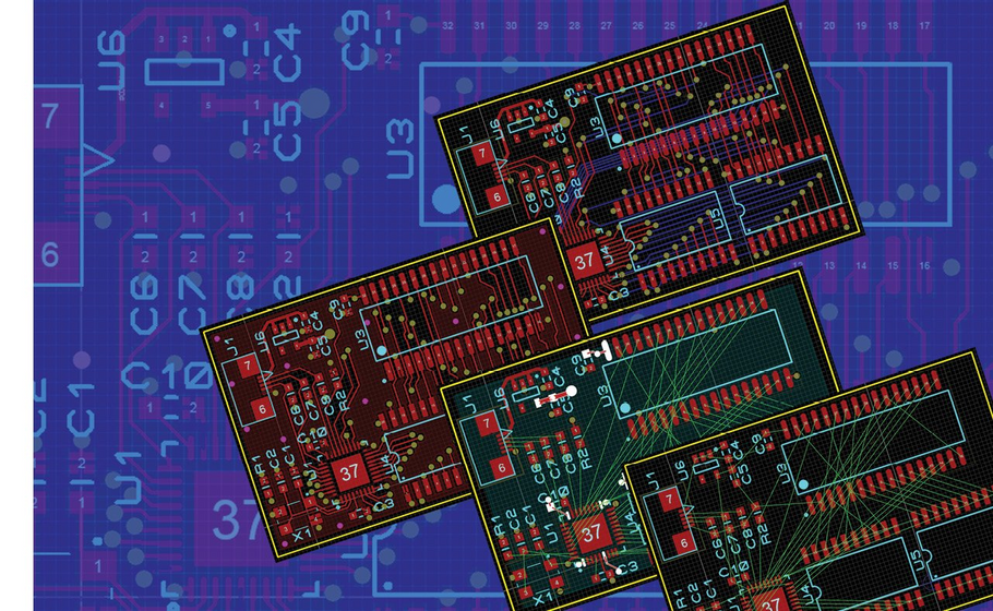
PCB Reverse Engineering

Manual PCB Reverse Engineering Process

PCB Impedance Design

How to make PCB with blind hole

Common Gerber files Problems and how to fix them?

Staggered Microvias and Stacked Microvias PCB

HDI board stack-ups

How are multilayer circuit boards made?

-
Previous
- Page 1 of 6
- Next