
Lily's Column
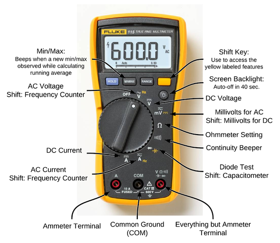
How to Use the Multimeter
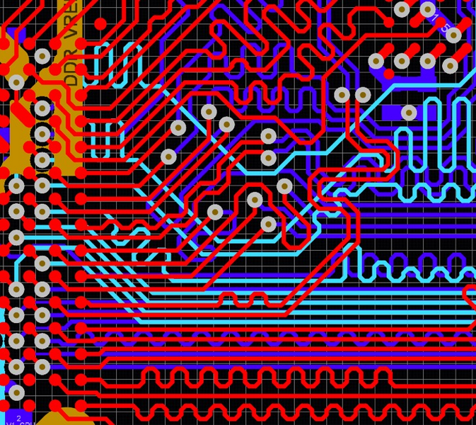
6 Layers impedance design
4 Layers impedance design

2 Layers Impedance Design
What affect PCB impedance and how to calculate impedance

Impedance Matching in PCB Design

What is Reflow Soldering?

What is Wave Soldering?

What is a HDI PCB ?

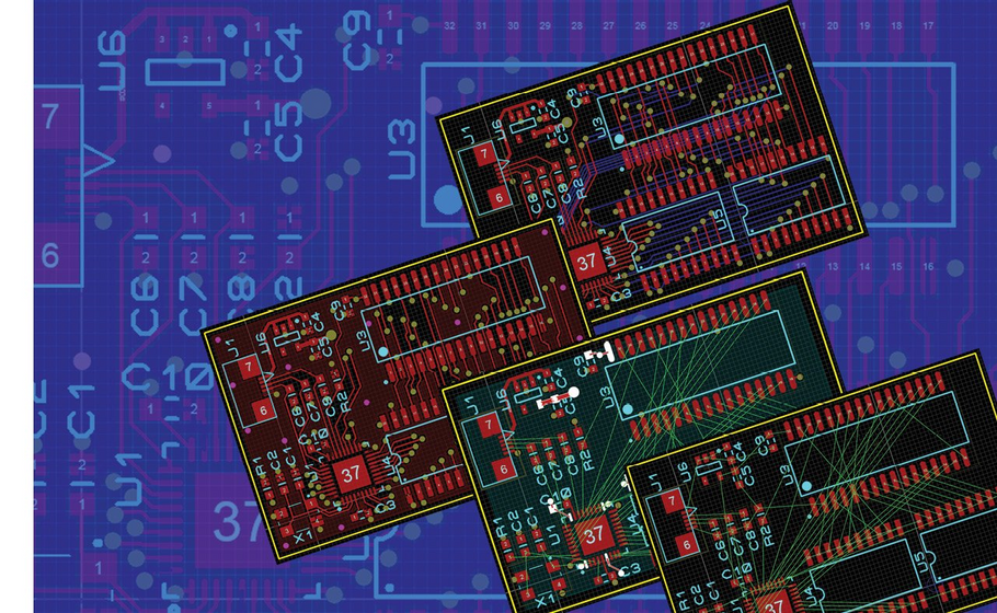
How to Reverse Engineer a Schematic From a Circuit Board

What is a capped via hole?

Integrated Circuit Manufacturing Process
