
Lisa's Column
Beginner’s Guide to Creating a Perfect PCB Layout Design

How to Calculate PCB Trace Width
Impedance Matching for USB Interfaces in PCBs

PCB Antenna Design Software Solutions

PCB Design File Formats Overview

The Ultimate Guide To PCB Trace Width Calculator

The Role And Design Guidelines Of PCB Ground Plane

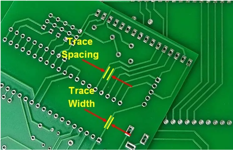
Trace Spacing: A Guide For PCB Design

Q: What is a PCB Copper Pour Area

Wireless Power Transmitter Reference Design

Routing Rules of BGA package in PCB design

How to Use PCB Trace Calculator for Printed Circuit Boards

-
Previous
- Page 1 of 8
- Next