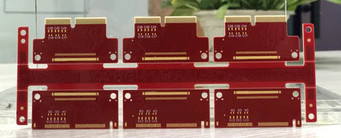
During PCB manufacturing, the solder mask opening size should be larger than the pads or copper areas desired to be exposed. Because of the skin effect, the PCB oil around the solder mask opening will gather, and the exposed area will be smaller. Usually, the width/length of the solder mask opening is 4mil larger than the pads.
Do you need to set up the solder mask opening size during PCB design? No, you don't have to. You just need to keep the same size as the required exposed pad/via size because the EDA tool will automatically enlarge the solder mask opening size.

