What is the best 6 Layer PCB Stackup?
The following is a set of typical 6-layer PCB circuit board stacks for reference.
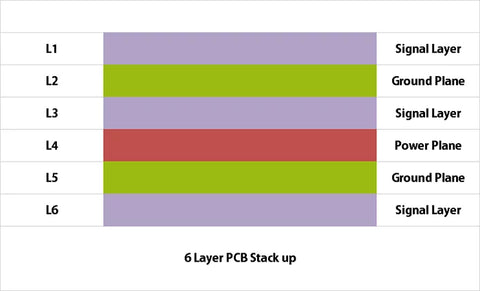
The structure is:
- Signal Layer
- Ground plane
- Signal Layer
- Power Plane
- Ground Plane
- Signal Layer
This may not be your most satisfactory 6-layer PCB stack structure because the signal layer in the circuit board does not have any shielding, and two of the signal layers are not adjacent to any ground plane. As signal integrity and performance become more and more important, such a 6-layer PCB stack structure has been gradually abandoned.
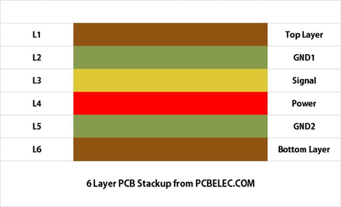
In this 6 layer PCB stack-up is the signal layers are reduced to 3 to add a ground layer:
- Top Signal Layer
- GND1
- Inner Signal Layer
- Power Plane
- GND2
- Bottom Signal Layer
This 6-layer PCB stack-up places each signal layer close to the ground plane to obtain the best return path characteristics. In addition, putting the power and ground planes adjacent to each other creates planner capacitance. But the same disadvantage is that you will indeed lose a signal layer for routing.
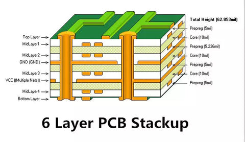
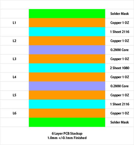
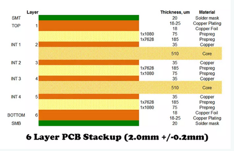
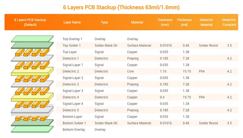
6 Layer PCB Stackup and Thickness
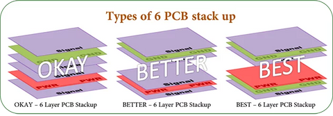
3 Types of 6 Layer PCB Stackup, the right one is best.
