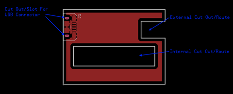
What we here mean with PCB milling is one of the manufacturing processes which is used to cut out the board contours and the slots or cut-outs inside the board. The slots or cut-outs are created through the milling process.
A PCB file usually contains several layers, and the mechanical layer is used to indicate the information about the PCB manufacturing and PCB assembly, such as the PCB dimension, dada sheets, vias information, special buildups, layer sequence, and assembly details, etc. The correct production of the overall size and inner holes depends on the mechanical layer. If you have multiple mechanical layers, there is always at least one to help you fabricate the board. PCB milling is processed according to the data in the mechanical layer.

Some considerations for PCB milling
1. A good result of milling depends on the accurate information in the mechanical layer. The data includes the exact board outlines with dimensions, the exact positions, and dimensions of all the internal milling and slots.
2. Don’t mirror or rotate the mechanical layer because all the layers are viewed from top to bottom. And do not scale the mechanical layer; the PCB dimension should be 1:1 reflected.
3. The routing and milling data are production-specific and depend on tool compensation, routing tools, routing order, and the orientation of each PCB manufacturer. Therefore, PCB manufacturers only require that all the routing and milling data are contained in the mechanical layer, then they will recreate the milling layer based on their manufacturing situation.
4. The standard tool size for all contour milling or slots milling is 2.0mm, which means the standard minimum radius of the inner corners is 1.0mm. You should indicate the requirement of the small inside corners in the mechanical layer before PCB fabrication.
5. Each PCB manufacturer may have different manufacturing tolerances. Please mark your specific tolerance in the mechanical layer or mention the tolerances with your PCB manufacturer separately.
