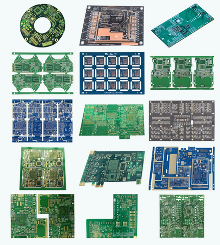
What is a HDI PCB ?

HDI stands for High-Density Interconnector. Thus, HDI PCB is a special type of PCB that has the capability of high-density interconnections. In simple words, it has more wires or conduction lines per unit area, utilizing the most out of the space and offering a compact PCB.

Contrary to the conventional PCBs, this PCB has tightly packed interconnections; thus, it saves a lot of space and offers more component density. Suppose a conventional multilayer PCB has ten layers for the implementation of a circuit and is about 5 inches x 5 inches in dimension. The same circuit can be implemented on an HDI PCB, and there will be fewer layers, could be eight layers or fewer. Moreover, the size of the board will also reduce. Thus, HDI PCB has the capability of making a circuit compact.

The world is moving towards more and more compact devices, appliances, and equipment. Everything is getting smaller and smaller day by day, and an important role in this regard has been played by HDI PCB. It has helped in achieving smaller designs of the products, faster processing, and other benefits, but everything comes at a high cost. HDI PCBs are more costly compared to other boards because of their exceptional features.

How is High-Density Interconnection Achieved? - Microvias

Conventional multilayer PCBs require plated through-hole (PTH) vias to create a connection between the layers. The vias take more space, and if space requirement is reduced, we can easily achieve high-density interconnection.

HDI PCB promises a high density of interconnection in the given area. This is because it uses special blind and buried vias. It uses micro vias that are drilled using a laser. The diameter of the laser beam is 1 Mil, so it can create a tiny via to save space. Due to the use of laser technology, this type of via has a very small diameter, nearly 0.006 inches (1.5mm) or lesser than that. Consequently, there are few layers in the PCB, and high-density interconnection is achieved.

Micro vias are created with extra precision, and they are more accurate compared to mechanical drilling. Due to the presence of micro vias, there is more space available on the boards, so there are more pin counts on the PCB. This ensures the placement of more components compared to traditional PCBs. Along with the benefit of space-saving, micro vias also bring many advantages, including faster signal transmission, low resistance and capacitance, and reduction in the weight of the final PCB.

The most important thing about micro vias is that they can be placed inside the pads of the surface-mounted components. These vias are quite small, so they can utilize the space under the pads. These vias are known as microvias-in-pad. They save a lot of space on the PCB as there is no need for a separate space to create micro vias. They can even be placed under the pads of fine pitch BGA components/packages.

Mircovias can be classified into various types.

  • Blind Micro vias: These vias start from the surface layer of the PCB and can connect several layers beneath it. It usually connects one or two layers to the surface layer.
  • Buried Micro vias: These vias are inside the PCB, and they connect the internal layers of the PCB. They do not connect the surface layer to internal layers.
  • Stacked Micro vias: The blind via can be stacked over a buried via. This is known as stacked micro via.