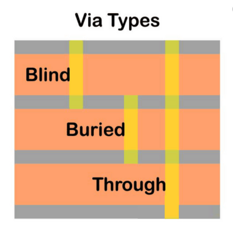
Regular vias are the copper-plated holes on a two-layers board, and they build a connection of the surface layers. This kind of via is named as a through-hole via. Through-hole vias pass through the entire board and connect all the layers. Vias are the solutions when the surface layer cannot meet all the connection demands.

Blind vias are the vias that can be seen from outside. They connect the surface layer to the inner layer (one inner layer or more), and will not go through the whole board.
Buried vias are the vias that cannot be seen from outside. They are “buried” inside the board and responsible for the interconnection of the inner layers (two layers or more).
The benefits of blind vias and buried vias
-
Firstly, blind vias and buried vias are often applied in HDI PCBs because they provide excellent power delivery and a high density of layer numbers. Blind vias and buried vias also allow more surface area due to they only go through necessary layers. They are usually used for fine pitch BGA components.
-
Secondly, Blind vias and buried vias are often used in the multi-layer PCBs (usually at least four layers). When the through-plated vias cannot meet the requirement of the manufacturing and performance, blind vias and buried vias can help to break the density limitation of traces and pads in a typical design.
-
Thirdly, blind vias and buried vias can improve the circuit density without increasing the board size and the number of layers, which results in smaller PCB volumes for high-density and high-performance PCB products. These vias technologies are more suitable for consumer electronics.
-
But blind vias and buried vias are much more expensive than standard vias, especially for the micro vias. Because these vias need more drill time and additional processes, even so, don’t forget to add them in your PCB design if you need a high-density PCB with compact size.
