Thicker Copper Board
Generally, printed circuit board copper thickness of more than 3oz is called Heavy Copper Board. Its thicker copper can conduct higher current and achieve better heat distribution. So, it is widely used in power electronic equipment, power supply system, and new energy fields, such as electric vehicles, voltmeters, and other emerging industries. One technology is indispensably used for the production of the thick-sopper PCB, and this technology is called "electrostatic spraying technology".
Electrostatic Spraying Technology
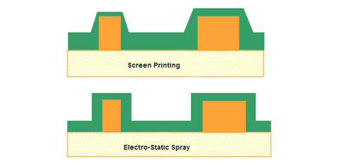
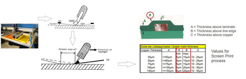
The biggest difficulty in the production of thick copper sheets lies in the process of a solder mask. The traditional screen printing process will make the thickness of the solder mask uneven, poor coverage, bubble, soldering fold, line corner oil accumulation, line edge exposure, and other appearance problems. This leads to lines not being protected with the best coverage. Let's look at the diagram below for the analysis of the traditional screen printing process: (it can be seen that at the two corners of line, B, the solder mask is very thin)
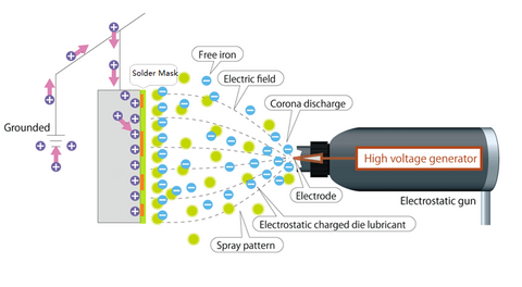
The PCB factory of PCBHERO uses the electrostatic spraying equipment imported from Japan, so there will be no such problem in the process of soldering. The working principle of the equipment is to spray soldering ink on the board in a dust-free vacuum environment. The schematic diagram is as follows:
Heavy Copper PCB Manufacturing Process
Compared with traditional soldering technology, no matter from the aspect of appearance, coverage (uniformity), adhesion force, surface hardness, electrical performance, resistance to hydrolysis attack, or from the perspective of industry acceptance standard IPC SM840, electrostatic spraying technology is undoubtedly the most advanced and perfect soldering process, which can maximize the quality of products.