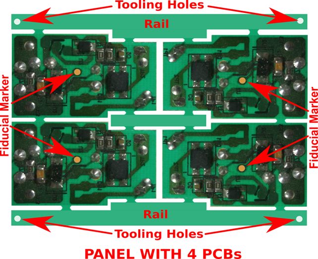
PCB Trace Technologies Inc. recommends designing boards with panelization in mind, as panelization offers significant advantages in efficiency for PCB manufacturing. To our customers this translates into higher manufacturing yield per panel, reduced lead times, better product quality, and reduction of cost per PCB.
A proper panelization scheme is one of the most important ways to improve the productivity in the PCB manufacturing process. The process is rather simple if you have the right PCB design software. However, for the uninitiated, a vital question is when to consider PCB panelization?
Although the benefits of panelization are realizable only during production, the effort must begin as early on as possible in the design stage of the PCB, that is, immediately after completing the PCB layout. It is best to consult the contract manufacturer at this stage, since each manufacturer is likely to have their own specific requirements as to how they would like their PCB array laid out for manufacturing.

Preparing for Panelization
As an eminent contract manufacturer, we at PCB Trace Technologies Inc. aim to maximize the customer’s gains from the benefits of panelization. Hence, we have listed some key points to help our customers prepare for panelization of their PCBs:
Panel Size:We use panels with standard sizes that our machines can handle. However, we are flexible about the size, and advise our customers on the most optimum size suitable to their order. If the order is a large production quantity, we advise the customer to go for the biggest panel size, as this offers the lowest unit cost. However, if the order is in small batches, we increase their ordering options by advising them to go for smaller panel sizes.
Board Shape:Ideally, rectangular shapes of individual PCBs work best for panelization, as it is possible to reduce wastage of material. Designers must convert unusually shaped boards by adding extra material around them to make their shapes rectangular. Most often, the operator will break off the extra material and discard it after assembly. CAD programs are a great help for panelization as they can rotate individual boards to fit the panel size in the most optimum way.
Array Strength:While panelization involves placing individual PCBs in a suitable array to arrive at a specific panel size, the designer must also keep in mind that after assembly the operator must depanelize and separate the individual boards. To make it easy for the operator to depanelize the boards, panel fabricators cut grooves around the PCBs, leaving them attached with webs at a few places, but weakening the strength of the array. Therefore, the designer has to tradeoff between maintaining the array strength and providing ease of separation for the operator.
Component Placement:Locating SMT components and/or copper tracks very close to the breakaway portion of the PCB can result in hairline cracks during the depanelization process. Likewise, connectors and other large components if overhanging a PCB can make it difficult for the operator when depanelizing.
Tooling Holes:These are non-plated holes placed on four corners of the panel. They help in orientation and alignment of the panel in machines during board assembly.
Fiducial Markers:These are recognition pads of copper, allowing the pick-and-place machines to orient themselves for each panel after loading. Fiducial markers increase the accuracy of SMT component placement for minor rotations and shift of the individual PCBs in the array.
Rails:To help with the conveyor handling during assembly, there must be at least two extra PCB material rails along the longer edges of the panel.
Tooling Equipment
To help with depanelization, operators generally use tooling equipment. The type of tooling equipment defines the gap between the boards, which is also important for defining the best possible array. The actual tooling process depends on the thickness and substrate material of the board.
For thin boards, PCB Trace Technologies Inc. uses either a router bit with a CNC machine or a laser cutter, as the boards cannot withstand the mechanical stress of standardized tooling equipment. For very thin boards, we must move the router bits at slow speed near the center of the panel to reduce the stress, and this can reduce the throughput.
For thicker and sturdier board material, we prefer using the manual or automated cutting methods using saws. We also place V-shaped grooves around the boards, while the operator uses a saw to separate them.
Immaterial of the method for separating the PCBs, we recommend using a suitable PCB design software package to allow placing fiducial markers and add spacing between the boards. We also strongly recommend our customers to contact their contract manufacturers when designing the panel to know how best to separate the boards, and the amount of clearance necessary on the panel.
Conclusion
Although panelization offers significant advantages, it can involve a new set of challenges also. Designers must take into account key design issues early in the design process. Consulting with the contract manufacturer early on at the earliest opportunity can help to avoid unnecessary redesigns and minimize waste. At PCB Trace Technologies Inc., we also take over the responsibility of creating panels for our customer’s PCBs.
