
PCB Schematic vs PCB Layout
PCB Schematic and PCB Layout are two crucial stages in the design of printed circuit boards (PCBs), and they serve different purposes in the process:
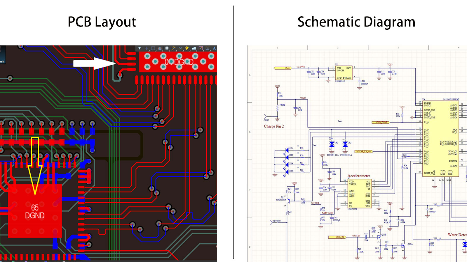
PCB Schematic:
-
Conceptual Representation: A PCB schematic is a symbolic representation of the circuit. It shows the electrical connections between components using abstract symbols for each component, such as resistors, capacitors, integrated circuits, and connectors.
-
Design Functionality: The main purpose of the schematic is to illustrate how the circuit works. It focuses on functionality rather than physical placement. Designers use the schematic to understand the electrical relationships and signal flow in the circuit.
-
Component Connectivity: It outlines the connections that need to be made on the actual board. Each line in a schematic represents a wire or trace that will exist on the PCB.
-
Reference Document: It serves as a guide for the layout process and as a reference for troubleshooting the PCB once it’s fabricated and in use.
-
CAD Software: PCB schematics are generally created using EDA (Electrical Design Automation) CAD software, allowing for easy editing and rearrangement of the circuit during the initial design phase.
PCB Layout:
-
Physical Realization: The layout is a detailed graphical representation of the physical placement of components on the PCB. It translates the schematic into actual traces on layers, component footprints, pad sizes, and other specific physical dimensions of the board.
-
Board Design: The layout process takes into account the physical constraints of the board, such as board size, layer stack-up, trace widths, and spacing for signal integrity, as well as placement for heat dissipation, and mechanical enclosures.
-
Manufacturing Blueprint: It generates the files needed for manufacturing the PCB, including the Gerber files or ODB++ files, which are used to fabricate the board and place components on it.
-
Routing: The layout process involves routing, which is the task of connecting all the component pins together with traces according to the guidelines provided by the schematic.
-
CAD Tools: Like the schematic, the layout is usually created using specialized PCB design software. Advanced tools provide auto-routing features, design rule checks (DRC), and interactive routing capabilities to ensure the board is free from errors.
Both schematic and layout are integral to PCB design – the schematic ensures that the circuit is electrically sound, while the layout is vital for the practical and manufacturable aspect of the PCB. A successful PCB design relies on the seamless transition from a well-planned schematic to an optimized physical layout.