
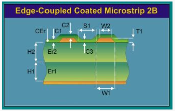
In the high-speed PCB design process, stackup design and impedance calculation are the first ladder to the top. The impedance calculation method is very mature, and the calculation of different software is not much different, which is relatively cumbersome. The "art of trade-off" between impedance calculation and process is mainly to achieve our impedance control purpose and at the same time ensure the process The convenience of processing and the reduction of processing costs as much as possible.
flow meter
Below we summarize some considerations for calculating the impedance of the stack design to help you improve the calculation efficiency.
1. The line width is better to be wide than thin
because there is a thin limit in the manufacturing process, and there is no limit to the width. Therefore, if the line width is thinned in order to adjust the impedance in the later stage and it hits the limit, it will be troublesome. Either increase the cost or relax Impedance control. Therefore, relatively wide means that the target impedance is slightly lower when calculating. For example, if the single-line impedance is 50ohm, we can calculate it to 49ohm, and try not to calculate it to 51ohm.
2. There is a trend in the whole
. There may be multiple impedance control targets in our design, so the overall impedance should be too large or too small. Don’t have situations like 100ohm being too large and 90ohm being too small.
3. Consider the residual copper rate and the amount of glue flow.
When one or both sides of the prepreg are etched lines, the glue will fill the etched gap during the pressing process, so that the thickness of the glue between the two layers will be reduced, and the residual copper rate will be smaller. , the more filled, the less left. Therefore, if the required thickness of the prepreg between the two layers is 5mil, a slightly thicker prepreg should be selected according to the residual copper ratio. 4. Specify the glass cloth and the glass cloth with different glue content. The dielectric coefficient of the prepreg or core board with different glue content is different. Even if it is about the same height, it may be a difference between 3.5 and 4. This difference can
cause
The single line impedance changes around 3ohm. In addition, the glass fiber effect is closely related to the size of the glass cloth window. If the design is 10Gbps or higher, and the laminate does not specify a material, and the board factory uses a single 1080 material, signal integrity problems may occur.
Of course, the calculation of residual copper rate and glue flow rate is inaccurate, the dielectric coefficient of new materials is sometimes inconsistent with the nominal, and some glass cloth board factories do not have materials, etc., which will cause the design of the laminate to be unable to realize or the delivery date to be delayed. Then the best way is to let the board factory design the stack according to our requirements and their experience at the beginning of the design, so that an ideal and achievable stack can be obtained in a few rounds at most.
This article is reproduced from: 51 Black Electronics Forum
Disclaimer: This article is a reprinted article, the purpose of reprinting this article is to convey more information, and the copyright belongs to the original author. If the videos, pictures, and text used in this article involve the copyright of the work, please contact the editor for processing.