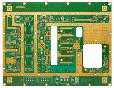
In electronics, we are still working with and developing different types of systems, but many aspects of electronic design are still being done separately. Although PCB system-level multi-board designs are now changing that.
Just as a single printed circuit board is designed with a block representing different circuit areas, the same approach can now be used to design entire systems. Traditionally, individual boards have been designed and manufactured to test their fitness and connectivity in the rest of the system. This slow and expensive process has now been replaced by a complete system design in a set of CAD tools. The key, of course, is to have the tools to support this level of multi-layer ECAD schematic system development. This is more information you should know about system design.

What is in the multi-board ECAD schematic?
The system design includes separate board development, which means that each board will still have its own schematic. What's new, however, is that you will also have system-level schematics. Each design will be represented in the system schematic, just as individual circuit hierarchy blocks are represented in the top-level table of a single PCB design. This will allow continuity between the boards to be checked, and each layout of the system will also be grouped together.
The multi-board schematic gives you a lot of benefits that you wouldn't get using the traditional personal board design process:
Each individual schematic design is linked to the top-level system design, allowing you to control system-level functionality from one location. This includes the system design and eliminates the need to use other tools or spreadsheets to manage these functions.
With each board represented in the system schematic, you can verify connectivity between each board through schematic design checks. This will allow designers to validate their in-system connections without first building and testing the hardware.
Along with the system schematic, the multi-board development process allows designers to check that each physical board design is consistent with the rest of the system. Using the 3D and mechanical co-design capabilities of layout software can greatly reduce the amount of prototyping required to detect mechanical conflicts.
The multi-board design process will help designers create all individual schematics and PCB layouts much faster than traditional individual design methods. This is because you can see in real time how all the different parts work together.
Multi - board schematic design skills
One of the things multiboard schematics should do in a complete system design is to modify your scope of thinking to the big picture. For veneer designs, most engineers are used to collecting and organizing materials before starting each design. Because multi-board designs will all be used in the same system, ways are sought to reduce the workload by organizing all the data together. For example, will the schematics use many of the same library symbols? If so, you can save a lot of time by developing libraries for system design collectively, rather than individually.
As you develop library parts for your entire system, look at some of the other design elements that also need to be organized. Will the boards be made by the same manufacturer? If so, work with your supplier to find ways to reduce production schedules and costs. Design rules are another approach that can be modified to improve efficiency. Rather than establishing rules and constraints for each individual design, they can be copied from design to design and modified as needed. Many design teams will keep libraries of design rules as well as engineering drawings and other types of documentation to improve efficiency.
Since the multi-board schematic design is an extension of the single design, you still need to complete all the individual schematic designs. These can be handled simultaneously by multiple team members while still maintaining their connection to the upper system design. However, take the time to make sure your design is complete by cleaning it up, adding all the necessary tags and text, and running a full design rule check. Most design teams have a checklist process to ensure that all these important details are done according to their company standards. The same inspection process should be used to ensure that the final system-level design is also complete.
, be sure to leverage all the capabilities of the design tool in system-level design. There's a lot more to do than you're used to in a single design, and you need PCB design tools that can handle the extra load.
Multi-board design and 3DECAD/MCAD co-design can realize the visualization of the whole system
PCB design tool for system schematics
To get the full benefits of creating multi-board system schematics, you need to ensure that the design tools support the entire process. The tools you need will be able to:
Enables you to complete system schematic design from top to single circuit board schematic. Your tool should recognize the connectivity between the boards electrically and represent the different boards at the top level.
Simulate the entire system. Yes, you still need to simulate the design of individual boards, but it's also important to be able to simulate circuits throughout the system, high-speed signals, and power transmission networks.
Display your PCB layout in 3D. It's not enough to just pass a regular design rule check; you also need to look at potential problems and obstacles that physical prototypes typically expose.
ECAD/MCAD co-design. After you have designed the complete system schematic, you need to see how the boards are installed and connected together.
