As sensors become more abundant in various end markets, the need for analog signal conditioning, including analog -to-digital converters ( ADCs ), continues to grow. The overall sensor market is expected to grow at a CAGR of over 9%. End markets include various Internet of Things(IOT) applications, factory automation and control, public health and safety, healthcare, and expansion in automotive. For ADCs , the market trend is toward higher-resolution, higher-speed devices as the cost of such solutions becomes more affordable.
As the name suggests, ADC drivers are specialized amplifiers designed to work with ADCs, including successive approximation, pipelined, and delta-sigma-based architectures.These specialized amplifiers are critical circuit components that enable ADCs to fully function , and will become even more important as higher-speed, higher-resolution converters scale.
Understanding ADC Inputs
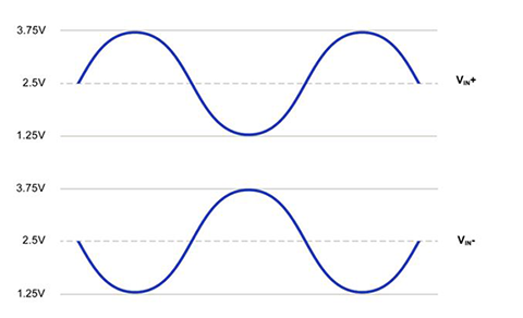
Before discussing the technical features required by ADC drivers, it is helpful to briefly outline the input architecture of today's ADCs. Differential signaling can be defined as two nodes having equal but opposite signals near a fixed point, called the common mode level. As shown in Figure 1, these two signal nodes are often referred to as positive and negative—or in-phase and out-of-phase.

Figure 1 This is what a differential sine wave looks like.Source : Microchip
In the above example, the full-scale input voltage is 5 V peak-to-peak differential and each leg swings 2.5 V peak-to-peak. The common mode level in this example is 2.5 V. Most of today's high performance ADCs use a differential input architecture because it provides better performance than single-ended inputs. These performance benefits include the ability to reject common-mode noise and common interfering signals and a 6 dB (or 2x) increase in dynamic range.
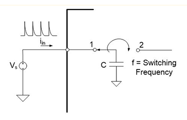
ADCs can present a particularly daunting challenge for system designers because they offer a variety of different input sampling architectures that must be considered at the system level. For the purposes of this discussion, the focus will be on ADCs that use switched capacitor structures for input sampling. In its most basic form, this input structure consists of a relatively small capacitor and an analog switch, as shown in Figure 2.

Figure 2 A simple switched capacitor input structure is used for input sampling. Source: Microchip
When the switch is configured in position 1, the sampling capacitor is charged to the voltage of the sampling node, in this case VS. The switch is then flipped to position 2 and the accumulated charge on the sampling capacitor is then transferred to the rest of the sampling circuit. Then the process starts all over again.
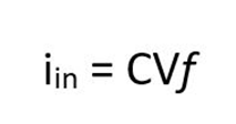
Unbuffered switched capacitor inputs, as described above, can cause serious system-level problems.The current required to charge the sampling capacitor to the appropriate voltage must be provided by an external circuit connected to the ADC input. When the capacitor switches to the sampling node (switch position 1 in Figure 2), a large amount of current will be required to start charging the capacitor. The magnitude of this instantaneous current is a function of the size of the sampling capacitor, the frequency at which the capacitor switches, and the voltage on the sampling node. This switching current can be described by the following formula:

where C is the capacitance of the sampling capacitor, V is the voltage on the sampling node (denoted VS in this example), and f is the frequency at which the sampling switch turns on and off. As shown in Figure 2, this switching current produces a high current spike on the sampling node.
The effect of this switching current must be considered when designing the analog circuit in front of the ADC . When the input current passes through any resistor , there is a voltage drop, causing a voltage error at the sampling node of the ADC. Distortion can also occur if the input node is not fully settled before the next sample period.
Solution: ADC Driver
Maintaining the required sensor signal integrity to take full advantage of these higher resolution, higher speed ADCs becomes very challenging. As the resolution and speed of the ADC increase, the effects of noise and distortion on the sensor signal become more pronounced. At higher ADC sampling speeds, care must be taken to ensure that the input signal has settled before the sampling event and that the higher bandwidth signal does not alias back to the signal bandwidth of interest.
To overcome these signal conditioning challenges, many ADC applications require an ADC driver that provides adequate stabilization and antialiasing. As mentioned above, most modern ADCs use a differential input architecture. One of the main functions of ADC drivers is to provide single-ended to differential conversion of input signals, although they can also handle differential input signals with ease.
Another function of the ADC driver is to buffer the input signal, thereby isolating the rest of the circuit from charge injection on the ADC input node. The ADC driver provides instantaneous charging to ensure that the sampling node settles within the tracking time, thereby minimizing any distortion associated with settling. Care must be taken with the board layout of the ADC driver and converter to ensure minimal trace resistance from the driver output to the ADC input.
Most ADC driver amplifiers also provide a hardware pin that enables the userr to level shift the common-mode voltage. This feature is ideal for ensuring that the resulting differential signal is within the ADC's input voltage range, maximizing dynamic range. As operating voltages continue to trend lower, dynamic range becomes more critical to ensure full resolution of the input signal.
Finally, like most amplifier components, the ADC driver can provide amplification and active filtering of the input signal. It should be noted that most ADC drivers have relatively low gain, typically only 1 or 2 V/V gain. By keeping the amplifier's closed-loop gain low, loop gain can be maximized, resulting in the lowest distortion. For example, if an amplifier has an open-loop gain of 100 dB and is configured for a closed-loop gain of 200 or 46 dB, there is only 54 dB of open-loop gain margin left to ensure linearity, or about a fraction of that in 500 . Therefore, a separate gain stage is usually placed close to the signal source to maximize the signal-to-noise ratio.
Getting the most out of ADCs
The popularity of sensors in various end markets has led to increased focus on signal conditioning circuits. Achieving this performance improvement becomes more challenging as the cost of high-resolution and high-speed ADCs continues to decrease.
To get the most out of your data converter, ADC drivers are critical for optimizing performance while adding negligible distortion, noise, and settling time error to the source signal. Specialized devices such as the MCP6D11 differential driver are designed to maximize the performance of high-speed, high-resolution ADCs.
Kevin Tret ter is a Senior Product Marketing Manager for Microchip Technology Inc.'s MSLD business unit.
