
PCB stack-up
What is a PCB stack-up?
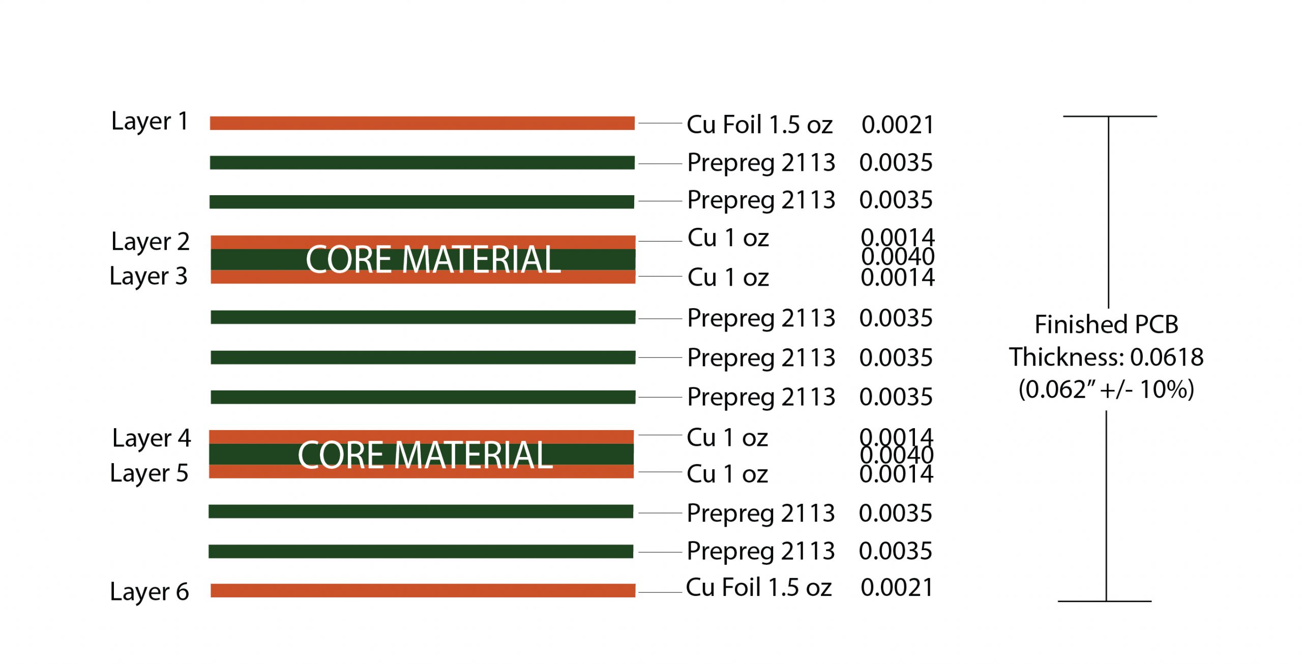
Stack-up describes the construction of a multilayer board in sequential order. It provides vital information like material thickness and copper weights required to fabricate a PCB. Stack-ups are also referred to as build-ups. The stack-up also gives the details of trace width for different controlled impedance traces such as 50ohms, 100ohms differential. An example of a 6-layer stack-up is shown in the above image.
What are the different layers present in a circuit board?
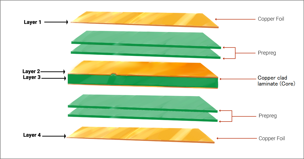
A stack-up primarily consists of metal foil, prepreg, and copper-clad laminate (core).
Metal foil: Copper is the most commonly used metal foil in PCB construction.
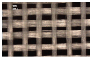
Prepreg: It is an interwoven glass cloth impregnated in epoxy resin. The resin is left semi-cured.
Copper-clad laminate: Single or multiple plies of prepreg bonded together along with the top and bottom copper foil makes a copper-clad laminate. This is also known as the core.
Power and ground layers in PCB stack-up
The power plane is a copper layer connected to the power supply. It is often designated as VCC in PCB design. The main function of the power plane is to provide a steady voltage supply to the PCB. In multi-layered boards, if a component needs to draw power then it is simply connected to the via that makes contact with the power plane. Similarly, the ground plane is a plane of flat copper connected to the common ground point in the PCB.
ADVANTAGES OF USING POWER/GROUND PLANES
- The power and ground pins of the components can easily be connected to the power and ground planes.
- It provides a clear current return path, especially for high-speed signals. This in turn reduces the EMI (electromagnetic interference).
- The power planes have a larger current carrying capacity than the traces. This also reduces the operating temperature of the PCB.
What is PCB lamination?
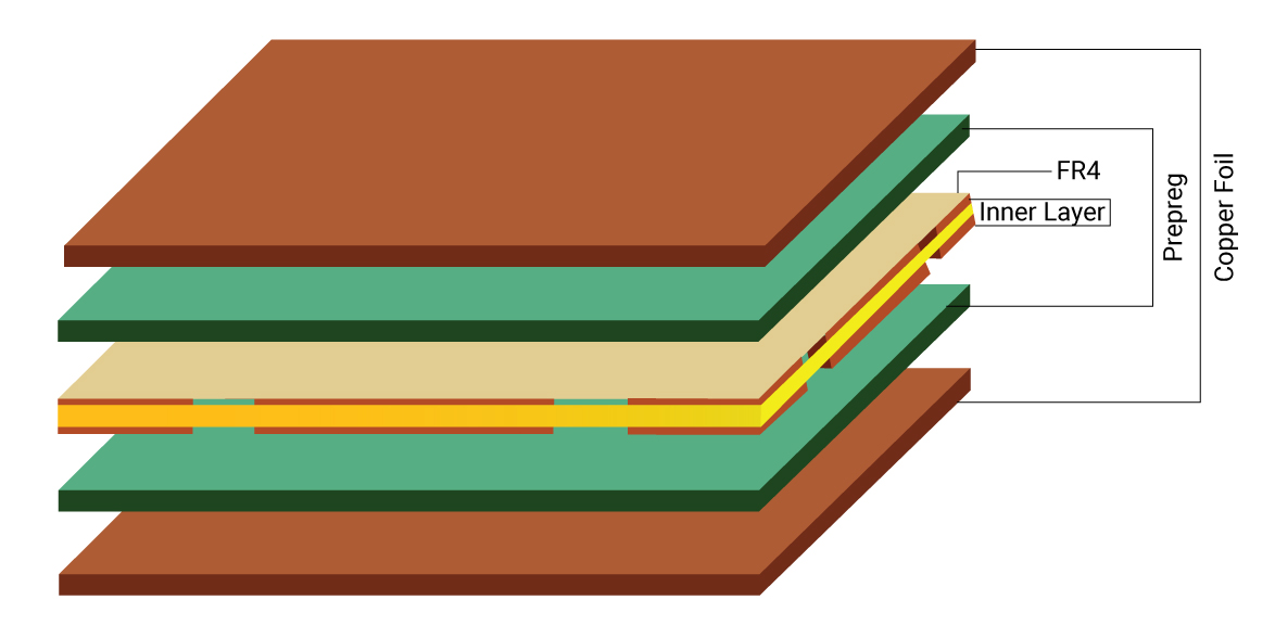
The lamination is the process of placing the stack-up under extreme temperature and pressure to bond prepreg and copper foil to the base PCB inner layers.