
Changes in USB 4: Data Rate and Signal Integrity
The new USB 4 specification allows for serial data transfer rates up to 40 Gbps (10, 20, or 40 Gbps) over differential pairs, which is a big change compared to earlier generations of USB. The standard also doesn’t change the connector or receptacle form factor, so it’s still easy to integrate a low-profile USB-C connector into new systems. The shielding effectiveness required in USB 3.2 Type-C-to-Type-C cables also applies to USB 4 cables.
Since cables can be reused and component footprints are unlikely to change, designers will not need to change their layout so much. At the cable level, connector level, and board level, the other changes in the specification relate to losses in the system (both insertion and return loss), allowed crosstalk, and skew in differential signal lines. Obviously, the components need to change, but the USB 4 standards also impose some stricter signal integrity requirements that need to be addressed during board design.
Total System Losses
Just like other high speed signalling standards, there are limits on allowed return and insertion losses. The USB 4 standard specifies these at multiple points in the system (connector/cable/PHY). The table below shows the loss budget under the USB 4 standard (10 and 20 Gbps variants):

Losses should stay within these limits. One nice change from USB 3.2 to 4 is the higher loss budget in the cable, which allows a 2 m USB 3.2-compatible cable to be used. The Gen2 standard will be the starting point for most systems that will make them compatible with Thunderbolt and DisplayPort products.
Insertion Loss, Integrated Return Loss, and Integrated Crosstalk
The USB 4 standards take a signal integrity approach I’ve advocated in an earlier article and set design requirements across the signal bandwidth, rather than at a single representative frequency. They also use this to define an ideal cable with insertion loss values at specific frequencies within the bandwidth. Insertion losses, reflection losses, and signal distortion in the system come from:
- IC die load, including pin-package inductance
- Connector and receptacle tongue Ohmic losses
- Dielectric absorption in the substrate, which depends on trace geometry
- Fiber weave effects (also introduces skew)
The one area that the PCB designer has control over is the selection of PCB substrate materials, properly sizing traces for defined differential impedance, and routing choices to prevent reflection, crosstalk and return loss. Sizing traces to minimize a specific metric over a broad bandwidth is a somewhat complex design problem in any context, and sizing differential pairs in USB 4 design is no different. Take a look at the article I’ve linked above for a discussion of this problem over broad bandwidths.
Specifically for USB 4, the metrics used to optimize entire channels in order to minimize losses and crosstalk are integrated metrics (these apply to Tx and Rx channels in the cable and on the board):
In the second equation (ITX) above, the S-parameter refers to multi-port S-parameters, i.e., it quantifies differential crosstalk between Rx and Tx lines. Minimizing these loss sources throughout the relevant signal bandwidth requires selecting a suitable upper frequency (usually 5x the Nyquist frequency for 2-level signals) and adjusting the trace geometry until the above functions are suitably minimized. There are some other routing guidelines that should be followed, which I’ll outline below.
USB 4 Routing Guidelines
There are some general high speed PCB routing guidelines that apply to USB 4, as well as some specific guidelines that must be followed:
- Set the differential trace geometry (width and spacing) such that the differential impedance is 80-85 Ohms (~40-42.5 Ohms single-ended impedance).
- For electrically short interconnects, adjust trace size to minimize return loss (make as negative as possible) while balancing low crosstalk. For long interconnects, try to adjust traces to get insertion loss within the loss budget shown in the above table.
- Follow the standard design guidelines and component selection for USB-PD devices.
- Use interleaved routing (Rx pairs between Tx pairs, see below) to reduce differential FEXT.
- Use 0201 passive components on Tx/Rx/terminations as these components have smaller parasitics.
- Consider zig-zagging traces and using a substrate with tighter glass weave to compensate for fiber weave effects.
- According to official documentation from USB-IF, traces in USB 4 PCBs should be routed with smooth bends rather than at sharp angles. Any-angle routing tools in your PCB design software let you route in this way.
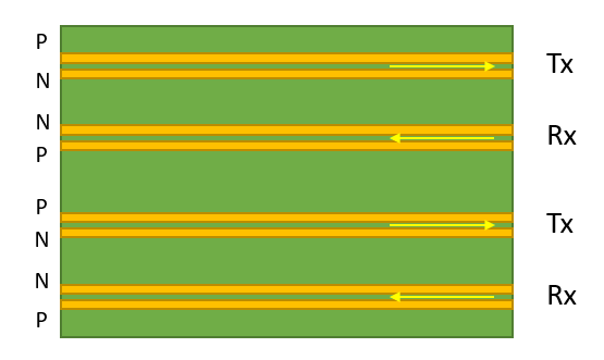
Interleaved routing should be used in USB 4