It is very important for digital PCBs to be carefully designed and engineered in order to eliminate problems like impedance discontinuities in transmission lines, improper plating of the through-hole interconnections, and other signal-integrity-related issues. Digital PCBs have a number of features that give them an upper hand during the functioning of an electronic circuit. Some of these features are:
- High layer count
- Tight dimensional tolerances
- Stub elimination
- High packaging density
- Complex stack-up structure, and more
Difference between Analog and Digital PCBs
There are various similarities and differences when it comes to analog and digital routing in PCBs in terms of bypass capacitors, power supply, ground design, voltage errors, electromagnetic interference (EMI), etc caused by PCB board routing.
Analog circuits consist of a combination of Op-Amps, resistors, capacitors, and other electronic components used on a PCB. These combinations of various components forming an analog circuit can vary in different manners. The main two applications of analog circuits are:
- Filtering signals: In the case of a continuous signal, a continuous analog filter is needed to remove all the unrequired frequencies from the circuit. As compared to a digital filter, analog filtering applications are much easier and more economical.
- Sensors: Converting adaptable real-world data into information that is recognizable by an embedded system or a computer is done with the help of sensors. If data is not available, sensors create an analog signal and convert it into digital signals. These systems have low amplitude and need signal conditioning in order to increase the quality of the signal to better utilize the full range of an ADC, unlike high voltage systems.
On the other hand, digital circuits consist of a combination of logical and sequential components by making use of logic gates that work on digital signals. When compared to analog circuits, digital signals operate on the logic of 0’s and 1’s to represent data in a digital form on a single IC.
Criteria for selection of PCB materials for Digital circuits
There are certain factors that should be taken into consideration while selecting materials for digital PCBs. Some of them include
-
Dimensional tolerance stability: The digital PCB must-have materials that will provide flawless mechanical stability while going through different temperature stability, vibrations, shocks, and electrical surges.
-
Superior thermal management: The materials must have the capacity to provide excellent heat transfer and heat dissipation, and must ensure the layers do not decompose, delaminate or start to peel away at higher frequencies
-
Enhanced signal performance: During the functioning of the circuit, the signal performance should be constant throughout the PCB with minimal signal losses even during frequency variations. Designers must make sure that the selected materials have a low dielectric loss factor (Df) to ensure that losses do not take place.
-
Tight impedance control: Digital PCBs will require tight control of impedance routing as they will have to maintain a stable dielectric constant (Dk) during high-speed operations.
- Moisture and chemical resistance: Materials that have a low absorption rate of moisture and chemicals must be selected so that there will be minimal variations in the desired electrical performance in the PCB.
Digital PCB materials
The foundation or the base of a PCB antenna consists of a substrate and a laminate, which also determines the performance of the PCB. Qualities such as function, longevity, and cost efficiency should be kept as a priority while designing a PCB, hence selecting the proper type of PCB material is critical. The material that one considers while designing a PCB can have a short-term or long-term effect on the performance. The pricing of a PCB material is directly proportional to the performance of the PCB. When the high performance of a PCB is not essential, a material named lightweight polyester can be considered as it comes with a low cost and good versatility
While selecting the materials, the temperature is a parameter that must be considered. The heat resistance should be higher than the heat produced as due to surplus heat a circuit may fail. Tg (glass transition temperature) is when PCB loses its rigidity and ability to perform well. Tg should match the assembly process being used, as a Tg with a minimum of 170° C is recommended for lead-free assembly. For a high-performance PCB, Tg should be higher than 170°C whereas a standard PCB has a Tg of 130°C. The advantage of having a high Tg is that there is a great ability to resist chemicals and moisture.
Materials generally used in PCB substrates range from FR-1 and G-10 to PTFE. Laminates are formulated from CTE, PTFE, CEM, and various other compounds.
-
FR-4: FR stands for “flame retardant” and it is widely used in standard boards. It comes with two Tg points, the first is 135°C and the second is 150°C-210°C which is applicable for high-density uses.
-
G-10: It is a high-pressure fiberglass laminate. G-10 and FR-4 are used as an insulator for electrical and electronic application.
-
PFTE (Polytetrafluoroethylene): PFTE can be a good choice in high-frequency, microwave, and high power boards as it comes with a Tg of 160°C and 280°C.
-
CEM-1, CEM-2, and CEM-3: They work well in high-density applications. The Tg offered by CEM-1, CEM-2, and CEM-3 is 122°C,125°C, and 125°C respectively
- Polymide- As a substrate it offers a Tg of 250°C or more for high power circuits. For flexible circuits, polyimide substrates should be preferred since FR-4 substrates are rigid. Polyamide substrates are slightly costlier than FR-4 substrates but offer high resistance to temperatures.
Rules for designing digital PCBs
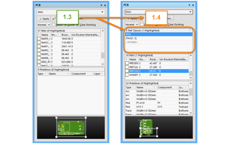
Most PCB design systems have the capability to transfer rules between the schematic and the layout. It permits the schematic to drive design rules instead of waiting to input all the constraints on the layout side, this is a huge advantage for designers. This level of organization offers designers the capability to form rules for specific net and component placing which are essential for circuit designing. Net or net class allows to group like nets together and assign a rule set to them. As the net rules are already present in the design database, so the designer need not rely on written instructions. For ensuring that the circuit board is designed precisely, here are some rules that need to be followed:-
- Default values- The design tool in the software will start off with default values which usually arise due to the leftovers from previous designs or system defaults. The designer should confirm these values before they start to ensure they aren’t routing with incorrect trace widths or placing the components too close. To avoid such problems, these default values can be reset through the settings. Also, it should be ensured that the spacing for default values is set as per the required schematic of the circuit to prevent inconveniences caused by prior settings.
- Classes - Although most of the rules can be configured for individual nets or components, this process can be time-consuming if there are hundreds of objects to work with that require unique rules and constraints. Some of the design tools provide a system for installing classes of nets and components to make it easier to configure rules and constraints.

Fig 2:- Installing classes
For example, the unique trace widths and the spacing requirements can be configured for a particular value of nets, a designer can create a set of rules for one power class and add those to nets.
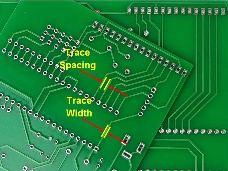
- High-speed design rules: When it comes to high-speed digital circuit designing, specific trace lengths can be set up as well as length matching can be done to nearby connecting traces which helps in improving the stability of data lines. In order to route the traces together at set differences, differential pairs can be set up at distances by creating unique trace topologies for specific net characteristics. For impedance-controlled routing, trace widths can be set automatically, and via sizes can be assigned to net classes.

Fig 3:- Trace designing
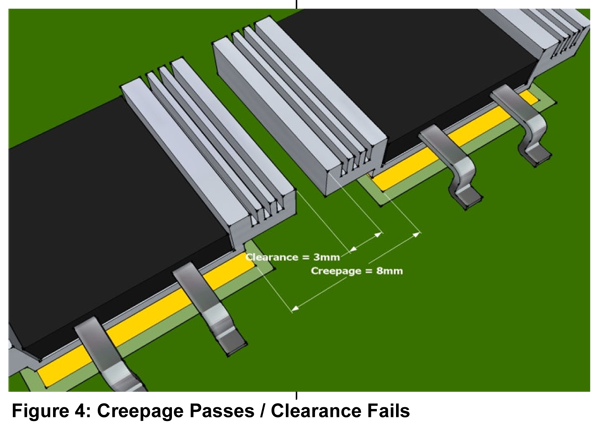
- Choosing the right PCB board spacing: Selecting the right spacing between the components used in the circuit and the spacing between the PCB lines helps in improving the desired electric output and also saves cost and rework. An ideal via aspect ratio of 6:1 ensures fabrication of the board wherever required which aids in trouble-free drilling.

Fig 4:- PCB spacing
Also, during the design process, components and circuit schematics must be properly represented in any CAD software which allows designers to view accurate simulations before mass production.
- Protection against electrostatic discharge: Digital PCBs are highly vulnerable to electrostatic discharge which may occur due to failure caused during the operation of solid-state components like integrated circuits (ICs), batteries, etc. If not taken seriously, circuits could malfunction or even explode. PCB designers must make use of ESD protectors like metal-oxide varistors, transient-voltage-suppression diodes, polymer-based suppressors, etc to avoid issues caused by electrostatic discharge.
