
Getting Started With RF Layout Guidelines
When you’re starting an RF PCB layout, there are some considerations that are typical for any board. How large is the board? Where do the critical components or connectors need to be located? How will it mechanically fit into its enclosure? These are all important questions for any PCB, but RF systems carry some unique design considerations that need to be answered.
Here are some of the important questions to answer when developing an RF PCB layout or a digital system with a high-frequency RF section:
- What protocols are involved? RF systems will need to do something involving high frequencies, which might be running at some standardized protocol and frequency range. There might also be more than one protocol in the system, and different protocols should not interfere with each other.
- What frequencies are involved? In general, lower frequencies are more forgiving than higher frequencies because parasitics are less noticeable at lower frequencies. RF systems are also less likely to couple radiated noise to each other at lower frequencies.
- What digital interfaces are involved? For some systems, the digital interfaces can have slower edge rates (SPI, I2C, etc.), so they might not have a major effect on analog performance unless you ignore best practices for routing and PCB layout. Embedded systems with high computing power will use high-speed protocols like gigabit Ethernet, DDR, PCIe, and others, which will more easily create crosstalk into an RF signal net.
Obviously, the term “high frequency” is subjective, but the important point is that the frequency will affect many design decisions in an RF PCB layout. Then there are system-specific requirements, such as you might see in a radar PCB or a system with MIMO antennas. The analog and digital sections need to be treated differently due to the way analog components interact with RF signals. This will then influence your component placement and routing choices in the layout.
Mixed-Signal PCB Floorplanning
Digital designers should approach an RF system with a floorplanning approach. The high-level goal here is to group components into functional blocks based on their role in providing functionality to the product. A side goal is to eliminate a situation where you need to route long RF interconnects all over the board to make the required connections.
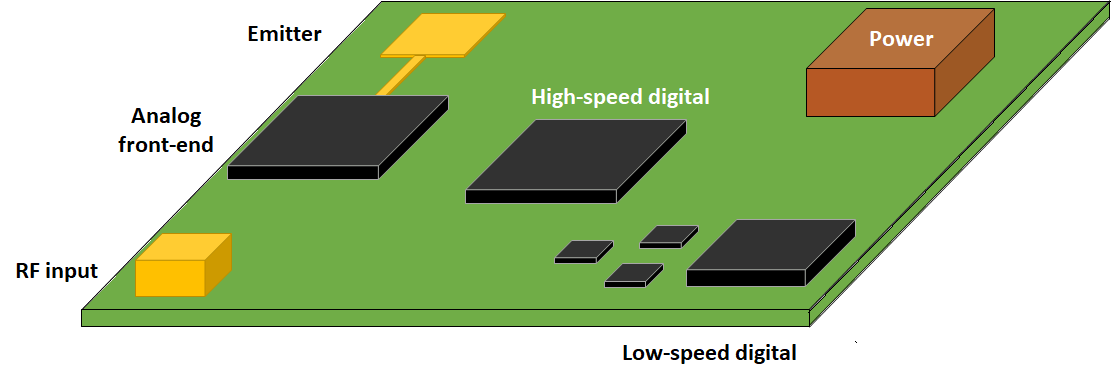
Try to keep things compact and segment things into different blocks where possible. When you start breaking up your functional blocks, you’re at risk of needing to route RF and digital traces back and forth across the board. This then creates more spots where strong crosstalk can occur, and it becomes more difficult to track your return path throughout the board. Floorplanning needs to be done alongside another important task: designing the PCB stack-up.
PCB Stackup Design for RF Devices
The stack-up design is related to floorplanning in that your routing strategy and layout will require a grounding strategy, especially at practical RF frequencies. The PCB stack-up you use will determine your power and ground access in the PCB layout, as well as available space for routing signals in your board. An example of an 8-layer count PCB stack-up you can use for an RF design is shown below. Although this is not typical, it provides the pattern for selecting layers and arranging signal vs. plane layers in the stack-up for low-speed, high-speed, and RF signals.

Example 8-layer stack-up with low-speed digital, high-speed digital, and RF signals on different layers.
In this example stack-up, there are traces on the top surface layer to provide direct connections between high-frequency analog components; these could be routed in any of the routing styles I’ll present below. Directly below this, we have ground/power planes, which are adjacent to provide interplane capacitance and to ensure stable power is delivered throughout the system (both for digital and analog components). In the internal layers, we can have other (lower frequency) RF signals, or we can have low-speed digital signals. On the bottom surface, I’ve allowed for the possibility of high-speed digital signals, although we could have these various signals mixed across the top and bottom layers as long as the return paths are controlled.
Plan Grounding to Support Routing
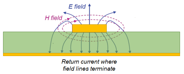
Grounding is important for defining a return path in an RF layout, although it’s better to think in terms of the space in the board occupied by traveling electromagnetic waves surrounding a trace. Note that the signal traveling on an interconnect does not appear as a flowing current on a conductor; this is a conceptual model that doesn’t match reality. The truth is that the electromagnetic field occupies some space around the conductor, and the strength of the field within this space will be determined by the presence of conductors around the interconnect.
The field around the trace then causes a return current to appear as a displacement current. This is because, if we look at the microstrip trace and ground plane arrangement shown below, we have two conductors brought to different potentials that are separated by an insulator (the PCB laminate material), forming a capacitor. The displacement current in the ground plane follows the electric field lines as they terminate at the ground plane.
Example 8-layer stack-up with low-speed digital, high-speed digital, and RF signals on different layers.
Why is this all so important for RF PCB layout? The reason is that placing ground near your high-frequency interconnects confines the field around the interconnect, and it ensures the return current stays closer to the trace at higher frequencies. Without the ground plane near a trace, we don’t know exactly where the return current will be, creating strong emission and reception of EMI.
To quickly summarize this point on grounding, we have two RF PCB design book guidelines:
- Don’t physically separate or split a plane layer into islands with digital and analog components and try to tie them together with a capacitor. You’ll have a poorly conceived return path that creates an EMI problem. Just use a single plane layer and learn to trace return paths.
- Take advantage of plane layers to ensure signal and power integrity. This means that, even if you have a simple RF board with only a few components, you’ll need at least a 4-layer board to provide the necessary plane layers.
Routing Your RF Traces
Now it’s time for the fun part: RF routing. All RF routing requires controlled impedance. This could require placing a termination network to ensure power transfer into a component (e.g., a divider or antenna), or placing a filter/amplifier to adjust specific frequencies traveling along an interconnect. Components that have an integrated RF output might have the required termination on-die, so be sure to check for this before placing any termination components at the driver end of your RF interconnect.
Trace Geometries
Once it’s time to route your critical RF traces, you’ll need to decide on a trace geometry. At Wifi frequencies and higher, most component application notes will recommend using a grounded coplanar waveguide to route your RF traces. However, it’s up to you as a designer to weigh the pros and cons of different trace geometries.
|
Routing style |
Characteristics |
|
Microstrip |
- Low isolation - Lower loss than other geometries, making them a better choice for longer links |
|
Stripline |
- High shielding due to nearby ground planes - Narrower than microstrips - Full loss experienced during propagation |
|
Coplanar waveguide |
- Moderate shielding due to nearby via fence and grounding - Full loss experienced during propagation - Requires a coupler design to ensure impedance matching at the input port - As simple to fabricate as microstrips and strip lines |
|
Substrate integrated waveguide |
- Highest possible shielding - Full loss experienced during propagation - Requires a coupler design to ensure impedance matching at the input port - Can be put through the PCB fabrication process, but requires more steps due to the use of via fence |
In all of the above geometries, we’re generally dealing with narrowband signals, and FR4 laminates tend to have quite low dispersion within narrow bandwidths you’d find in practical wireless/RF signaling standards. The one exception I can think of at the moment is software-defined radio, which requires the same approach to designing a target impedance as traces for digital traces (i.e., a wideband approach). Aside from this application area, you can generally ignore FR4 dispersion and you’ll get an accurate impedance calculation with a field solver as long as you know the Dk and loss tangent values at your target frequency.
The Impact of Trace Length and Vias
I bring up trace length and vias on RF interconnects because they can have similar effects on the total loss and signal distortion in an RF PCB, but not in the same way. Some designers will state that you should always use the shortest possible trace lengths on high-frequency signals, but they don’t seem to quite understand why it’s important. Loss is a factor, but so is input impedance, which is particularly important in termination networks and interconnects with coupling capacitors.
In short, there is a list of RF layout guidelines to follow regarding trace lengths and via counts on interconnects:
Traces between components in RF circuits, such as passives in a filter, can behave as transmission lines, even if routing between traces is short.
- Losses are important, but losses on short interconnects are dominated by return loss, which is due to a mismatch between two impedances. The mismatch needs to be dealt with by designing to accurate impedance, normally with a field solver.
- If you designed a microstrip with controlled impedance, then route it as a microstrip. Don’t route a microstrip as a coplanar waveguide because placing ground pour and vias around a microstrip will modify its impedance.
- Vias can start to act like filters or resonators at high frequencies, such as through-hole vias as at mmWave frequencies. Don’t route through too many vias as losses will add up, and don’t leave via stubs on high-frequency transmission lines.
- Follow other standard routing guidelines for high-speed/high-frequency PCBs to ensure you’re maintaining impedance and minimizing losses/distortion. I’ll discuss routing more in a future article.