STM32F103C8T6 Core Board – Schematic and PCB Design
STM32F103C8T6 Project Description
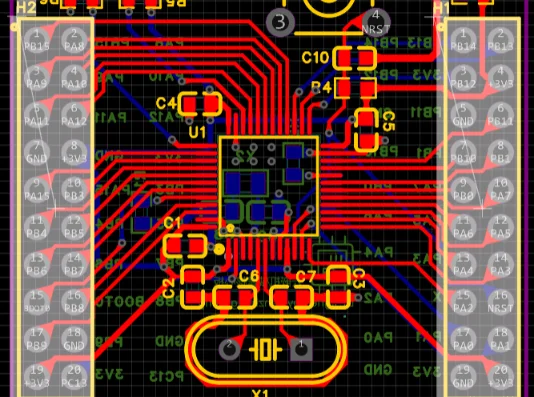
This project uses the official ST STM32F103C8T6 chip and designs a minimal system board, which can be easily expanded and used with the baseboard.
- Designed circuits include BOOT circuit, decoupling circuit, crystal oscillator circuit, SWD download circuit, reset circuit, power indicator circuit, and peripheral IO port circuit.
- The board is powered through external connections to the +3V3 pin and GND pin. It is recommended to power the board within the range of 3.3V to 3.6V, and it’s best not to exceed 3.6V power supply.
- A +3V3 power indicator circuit is designed to conveniently indicate whether the power input is normal.
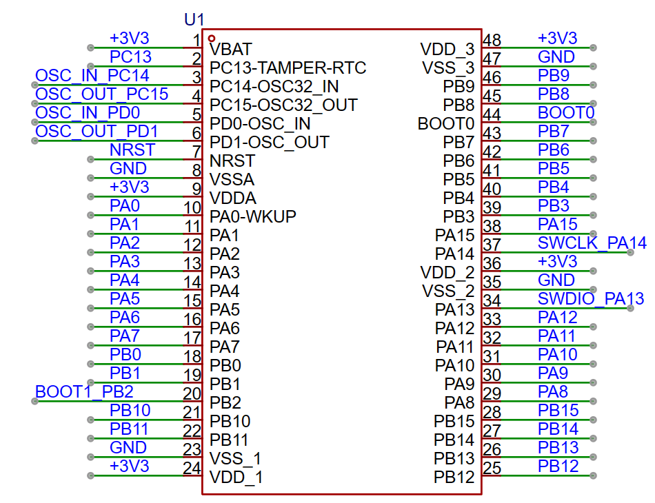
STM32F103C8T6 Pinout
Decoupling Circuit
Schematic Diagram
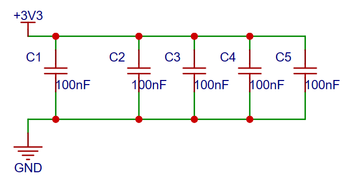
Placing a 104 (0.1μF) capacitor on the power pins effectively suppresses noise on the power supply, which is known as decoupling the power supply noise.
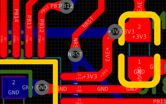
The closer the “Power – Decoupling Capacitor – Ground” points are, the better the decoupling effect.
For capacitors of the same material, even if the capacitance decreases to 1/10, the decoupling effect does not change significantly. For high-frequency decoupling, capacitors with the same package, capacitance values of 0.01μF, 0.1μF, and 1μF show similar results.
Surface-mount (SMD) capacitors have better decoupling effects than through-hole capacitors with the same capacitance due to the larger equivalent inductance of the through-hole capacitors, which affects the decoupling effect.
The capacitor with the smallest capacitance has the highest resonance frequency and the smallest decoupling radius. Therefore, it should be placed closest to the chip.
Capacitors with slightly larger capacitance can be placed slightly farther away, and the largest capacitance should be placed on the outermost layer. However, all capacitors for decoupling this chip should be placed as close to the chip as possible.
For high-speed PCB designs, it’s better to place capacitors on the same side as the chip for better decoupling. For MCU-type decoupling capacitors, there isn’t a significant difference between placing them on the front or back side.
PCB Design
Crystal Oscillator Circuit
Schematic Diagram
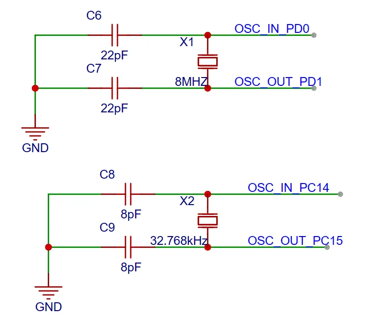
The STM32 has three internal clock sources, but the clock tree of the 32-bit chip requires five clock sources. Therefore, the PCB needs to accommodate external high-speed and low-speed clocks.
High-speed external clock can be a quartz/ceramic resonator or an external clock source, with a frequency range of 4MHz to 16MHz. A common choice is an 8MHz crystal oscillator for the main system frequency.
Low-speed external clock is a quartz crystal with a frequency of 32.768kHz, used for driving the RTC clock.
PCB Design
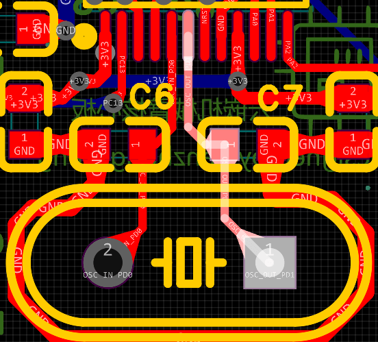
Notice that the area around the crystal oscillator is surrounded by GND traces, and it’s advisable to add vias on these GND traces. This is done to isolate the crystal oscillator. Also, avoid running traces on the top and bottom layers of the area where the crystal oscillator is located, as it can impact signal integrity.
Furthermore, the two capacitors near the crystal oscillator should be symmetrically placed.
SWD Download Circuit
Schematic Diagram
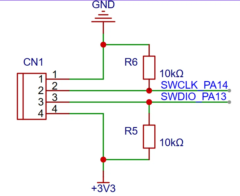
Introduction to JTAG:
We commonly use the Jlink downloader, which has a disadvantage of using the Jtag 20PIN interface. The excessive number of pins can lead to crowding on small PCB boards and increase wiring complexity.
Using the SWD interface for downloading and debugging requires only 4 pins: GND, RST, SWDIO, SWDCLK. The download speed can reach up to 10M/s, providing clear advantages.
SWD Mode:
SWD mode is more reliable than JTAG in high-speed scenarios. In situations with large amounts of data, JTAG program download can fail more frequently compared to SWD, which has a lower failure rate. Generally, if your emulator supports JTAG simulation mode, you can directly use SWD mode, as long as it supports it.
PCB Design

Power Indicator Circuit
Schematic Diagram

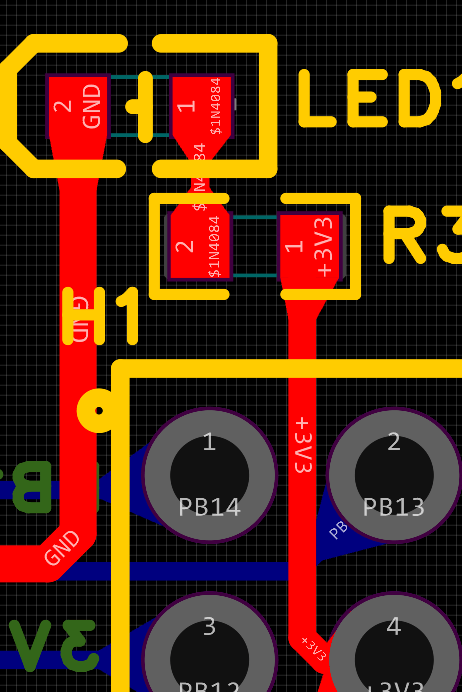
According to the datasheet, the maximum forward voltage drop is 2.4V, with a typical value of 2.1V. So, when the LED is operating normally, the maximum voltage drop across the LED is 2.4V. In this case, the voltage division across R3 is 0.9V.
Usually, LEDs light up normally at currents ranging from 3mA to 10mA. The maximum rated current is 20mA. Within the rated current, the higher the current flowing through the LED, the brighter it shines.
Here we choose I = 10mA, so R3 = U / I = 0.9V / 10mA = 90Ω. Since 100Ω resistors are more common in our materials, we can use a 100Ω resistor instead.
PCB Design
Reset Circuit Design
Schematic Diagram
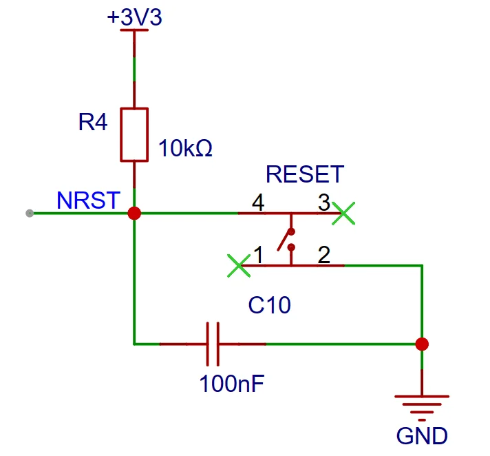
When the NRST pin is pulled low, a reset signal is generated, allowing us to perform a reset operation on our microcontroller.
In the circuit diagram:
– When the microcontroller is powered on again, capacitor C14 charges and conducts. The RESET voltage is low, causing a system reset. After a certain period, when capacitor C9 finishes charging and disconnects, the RESET voltage becomes high, and the microcontroller remains stable without resetting.
– When the button is pressed, it remains conductive for 20~50ms, connecting nRST to ground, resulting in a low voltage and a system reset.
PCB Design
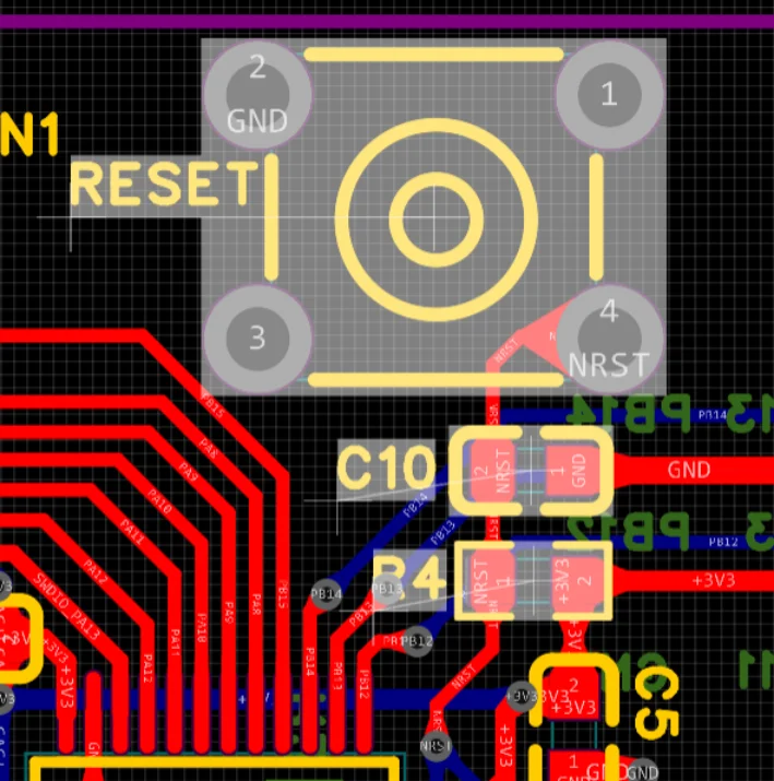
BOOT Circuit Design
Schematic Diagram

BOOT0 and BOOT1 of the STM32 control the chip’s boot mode, supporting internal FLASH booting, system memory booting, and internal SRAM booting. Specifically:
- User Flash: The chip’s built-in Flash.
- SRAM: The chip’s built-in RAM area.
- System memory: A specific area within the chip where a bootloader is preloaded during manufacturing. This is often referred to as an ISP program.
- ISP programs usually communicate via USART1.
When debugging and downloading programs using JTAG or SWD, the program is usually downloaded to the Flash. In this case, you can set BOOT0 and BOOT1 pins to low.
A 10K resistor is used because BOOT0 and BOOT1 are in a high-impedance state without external devices. The 10K pull-up and pull-down resistors serve as good current limiters and also protect the internal IC chip.
PCB Design
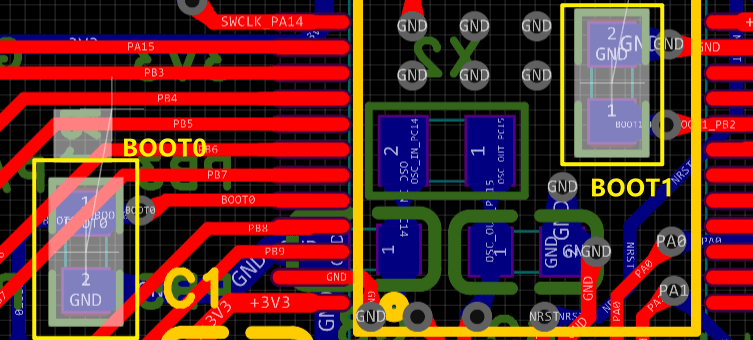
Here, we place the pull-down resistors for BOOT0 and BOOT1 on the back of the PCB to avoid interfering with our traces.
Peripheral IO Port Circuit
Schematic Diagram
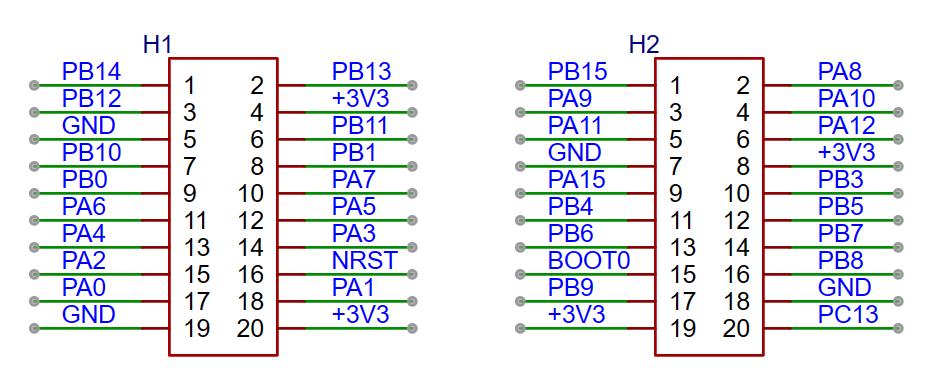
Unused pins are commonly led out using pin headers. It’s recommended to use double-row pin headers to enhance stability and minimize bending during insertion or removal, avoiding single-row pin headers.
Additionally, it’s advisable to lead out BOOT0. This facilitates the later design of a one-button ISP download circuit, allowing program download with a single USB cable.
Lastly, it’s recommended to lead out at least two sets of +3V3 and GND pins, so that each side of the pin header has a power supply, facilitating PCB wiring.
PCB Design
