I am designing a PCB using the NRF52832 and this antenna. The antenna design guidelines suggest ground clearance and direct traces from the NRF52832 to the antenna without the use of vias. However, due to size constraints on the PCB it is difficult for me to route the antenna without vias and ground plane.
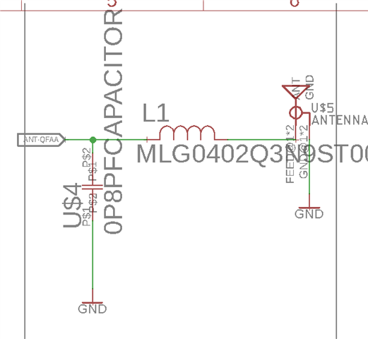
Above is the schematic I am using with a matching circuit using a 0.8pf capacitor and 3.9 nH inductor as suggested by Nordic

Above is the schematic I am using with a matching circuit using a 0.8pf capacitor and 3.9 nH inductor as suggested by Nordic
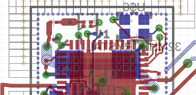
Above is a picture of the PCB layout. The blue striped trace that runs through the middle of the board is the trace from the antenna.
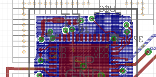

Above is a picture of the PCB layout with the ground and vcc plane.
What type of effect will the ground planes and vias have on the signal. I do not mind loss in range as I am communicating with a device only 1 - 2 meters away. What is the suggested solution for cases where clearance space is limited?
