Advantages of Coin Technology for Effective Thermal Management
We see a greater need for effective thermal management and significantly higher Radio Frequency performances for PCBs and subsystems; at the same time, these systems are required to decrease in size and still offer greater functionality than ever before. Constraints like these are often most acute in applications where Size, Weight, and Power are high priorities, such as in defense, aerospace, medical, and other sensor applications, and typically include RF power amplifiers, Tx/Rx modules, and phased array modules. There are various methods of thermal management - “Coin” technology versus traditional thermal technology.
One option to improve thermal conductivity is by increasing the plated via holes thickness.
Thicker copper walls can provide better conductive surface area, which can dissipate heat flux effectively. This can be particularly useful for high-power applications or for components that generate a lot of heat.
However, simply increasing the plated via hole side walls thickness may not always be the best solution for improving thermal conductivity in a PCB, where high-power amplifiers or high-density components are implemented on PCBs. Other factors, such as the choice of materials, board layout design, and component placement can also have a significant impact on the thermal performance of the sub-system or board.

Copper Coins Offer Superior Thermal Management
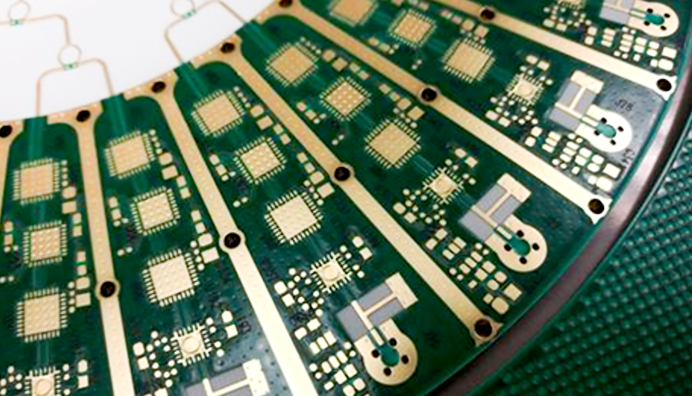
A more effective approach is to use copper coins that are integrated into the circuit’s structure.
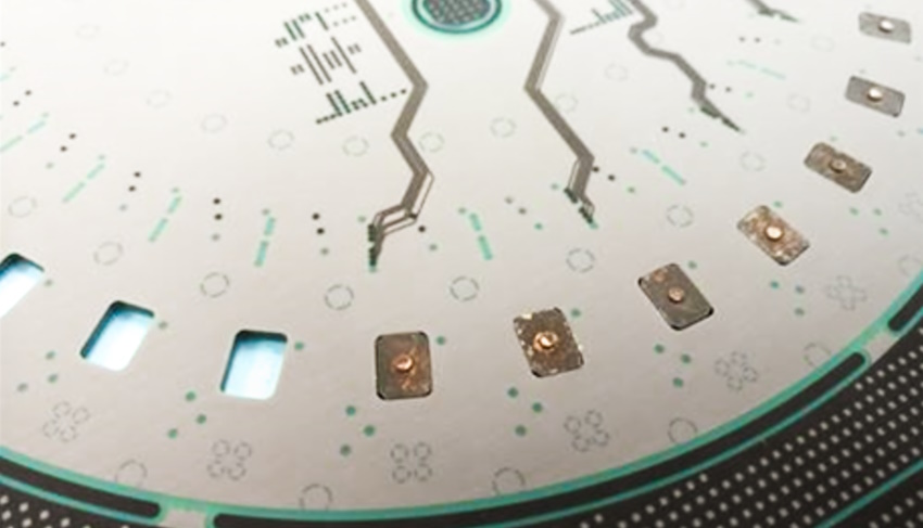
The copper coin is simply a piece of solid copper inserted into the PCB, typically under the component which needs cooling. The copper coin can provide at least 5 times the cooling compared to a via farm. The copper coin can provide direct contact between the heat-generating component pad to the heat sink of the subsystem, actually, the heat generated by the component on the PCB is conducted to the copper coin and then the heat is transferred to air or heat sink. The embedded copper coin is embedded in the PCB slot after routing and plated with the final finish process after PCB lamination.
Embedded copper coins are widely used and meet the heat dissipation requirements of high-power components by using the low thermal resistance of copper coins.
According to the design of the PCB, there are a few methods for embedding copper coins, as part of the PCB, as a sub in inner layers, or as a via farm replacement replacing a via hole form factor.
The embedded copper coins are inserted into the PCB slot after routing and metalized after PCB lamination. The coin is mechanically connected to the board by either mechanical pressure and direct contact with side slot plating or by using the prepreg flowing to the slot. The electrical connection is then established.
Choosing a coin technology is part of the detailed subsystem design and the embedding technology is part of the mechanical structure and the thermal design considerations. Pressing a coin in a slot is used when there is low vibration and low thermal stress. Laminated coins in different structures are used when higher thermal stresses and harsh environmental conditions are taken into consideration.
Overall, copper’s thermal conductivity is on average -200-300 times better than any conductive dielectric prepreg out there.
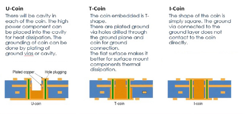
There are three types of coins that refer to the shape of the coin T-coin I-coin U-coin.
Choosing one of them will be according to the component that the HW designer is choosing for a specific design.

A drop-in package will require a U coin, an SMT package a T coin for very high power or an I coin when lower power is in use.
Complex Metal-Cored Circuit Solutions
A more complex solution is metal-cored circuits. These can be useful when the HW designer has to take high-power components, reduce the number of thermal resistance, mechanical, and adhesion layers, and use the metal heat sink as part of the sb system mechanical design. Heat transferred from components to the heat sink can either be transferred through thermal vias or by direct contact through cavities within the circuit that the components are mounted on. It is highly recommended to design the module or sub-system heat management solution prior to the specific board design as the heat flux must be removed from the heat sink as part of the whole solution. Typically, when using heat sinks the connection to the chassis is done by using a mechanical connection to the system using screws or pressured connection to chassis side slots. Overall, the thermal solution of the system is also critical to the design you choose, whether using conduction or convection will define the need in the heat sink, coin, or via farm.

