
How does an Inverter Work?
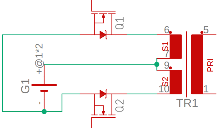
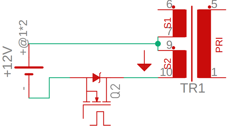
The basic schematic of the inverter circuit is depicted above. A positive voltage is connected to the middle pin of the transformer, acting as an input. The two other pins are linked to MOSFETs, which function as switches.
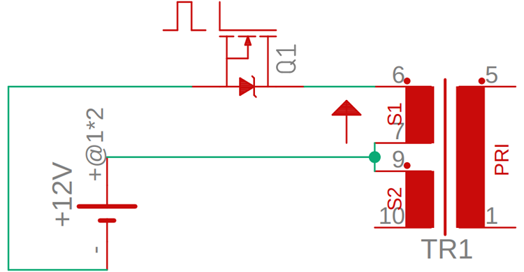
Enabling MOSFET Q1 allows current to flow in one direction, inducing magnetic flux in the transformer's core and producing a 220V output. Disabling MOSFET Q1 and enabling MOSFET Q2 reverses the direction of the magnetic flux, generating the desired output. This process, repeated 50 times per second by toggling both MOSFETs, creates an oscillating magnetic flux, inducing a voltage in the secondary coil as per Faraday's law. This is the fundamental working principle of an inverter.
Inverter IC TL494
Before constructing the circuit using the TL494 PWM controller, let's understand how the TL494 works.
The TL494 IC comprises 8 functional blocks, outlined below:

5-V Reference Regulator: The REF pin (pin-14) provides a stable supply for internal circuitry, including the pulse-steering flip-flop, oscillator, dead-time control comparator, and PWM comparator.
(Note: The reference is internally programmed to an initial accuracy of ±5%, maintaining stability over an input voltage range of 7V to 40V.)

Oscillator: This block generates a sawtooth wave for various control signals, and the oscillator frequency can be set using timing components RT and CT.
(Note: The oscillator frequency is equal to the output frequency only for single-ended applications.)

Dead-time Control Comparator: This block controls the minimum dead time or off-time, affecting the duty cycle of the output wave without tweaking error amplifiers.
(Note: An internal offset of 110 mV ensures a minimum dead time of 3% with the dead-time control input grounded.)

Error Amplifiers: High-gain error amplifiers receive bias from the VI supply rail, permitting a common-mode input voltage range from –0.3 V to 2 V less than VI.

Output-Control Input: This input determines whether the output transistors operate in parallel or push-pull mode.

Output Transistors: The IC has two internal output transistors in open-collector and open-emitter configurations, capable of sourcing or sinking a maximum current up to 200mA.
Features of TL494 IC
- PWM power-control circuitry
- Uncommitted outputs for 200-mA sink or source current
- The ability to select single-ended or push-pull operation
(Note: Information on the internal schematic and operations is derived from the datasheet, with some modifications for clarity.)
Components Required

TL494 Inverter Circuit Schematic

TL494CN Inverter Circuit Construction
For this demonstration, the circuit is assembled on a homemade PCB, using the provided schematic and PCB design files. It's crucial to note that connecting a substantial load to the transformer output can lead to a significant current flow through the PCB traces, potentially causing them to burn out. To mitigate this risk, jumpers have been included to enhance current flow.