About P55NF06 MOSFET
P55NF06 is an N channel power mosfet transistor that is commonly used in electronic circuits to control the flow of current. It has a voltage rating of 60V and a current rating of 55A. This MOSFET is widely used in various applications such as voltage regulators, power management circuits, inverters, and motor control circuits.
Features
- Low gate charge
- Fast switching speed
- Low input capacitance
- Excellent thermal performance
- N-channel enhancement mode power MOSFET
- Designed for high-current, high-speed switching
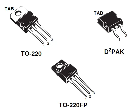
- Multi package: TO-220, D²PAK, TO-220FP

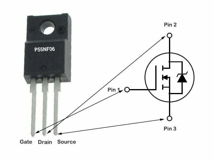
Pinout Configuration

| Pin Number | Pin Name | Description |
|---|---|---|
| 1 | G | Gate - This pin is used to control the flow of current between the source and drain. By applying a voltage to the gate, the MOSFET can be turned on or off. |
| 2 | D | Drain - This pin is connected to the load or circuit that you want to switch or control using the MOSFET. When the MOSFET is turned on, current can flow from the source to the drain. |
| 3 | S | Source - This pin is connected to the ground or negative terminal of the power supply. When the MOSFET is turned on, current can flow from the source to the drain. |
Technical Specifications
| Parameter | Content |
|---|---|
| Model | STP55NF06 |
| Package | TO-220 FP-3 |
| Lot Number | 19+ |
| Manufacturer | STMicroelectronics |
| Product Type | MOSFET |
| RoHS | Yes |
| Mounting Style | Through Hole |
| Number of Channels | 1 Channel |
| Transistor Polarity | N-Channel |
| Vds - Drain-Source Breakdown Voltage | 60 V |
| Id - Continuous Maximum Drain Current at Tc = 25 °C | 50 A |
| Rds On - Drain-Source On-State Resistance | 15 mOhms |
| Vgs - Gate-Source Voltage | 20 V |
| VGS(th) - Gate-Source Threshold Voltage Vds | 3 V |
| Idm - Pulsed Drain Current | 200 A |
| Qg - Total Gate Charge | 44.5 nC |
| Minimum Operating Junction Temperature | -55 C |
| Maximum Operating Junction Temperature | +175 C |
| Pd - Power Dissipation | 30 W |
| Configuration | Single |
| Channel Mode | Enhancement |
| Height | 9.3 mm |
| Length | 10.4 mm |
| Series | STP55NF06FP |
| Transistor Type | 1 N-Channel |
| Width | 4.6 mm |
| Forward Transconductance - Min | 18 S |
| Fall Time | 15 ns |
| Rise Time | 50 ns |
| Typical Turn-Off Delay Time | 36 ns |
| Typical Turn-On Delay Time | 20 ns |
| Unit Weight | 2.040 g |
Application
- Power supplies
- Voltage regulators
- Motor control circuits
- Audio amplifiers
- Solar inverters
- Battery management
- EV charger
Operating Principles of P55NF06 MOSFET
The P55NF06 is a type of Power MOSFET (Metal Oxide Semiconductor Field Effect Transistor) that is commonly used in power electronics applications. Here are some of its operating principles:
The P55NF06 MOSFET is a P-channel device, meaning that the channel is formed by positively charged carriers (holes) in the semiconductor material. When a positive voltage is applied to the gate terminal, it creates an electric field that repels the holes in the channel, causing the channel to become less conductive.
The drain current of the MOSFET is controlled by the voltage applied to the gate terminal. When the gate voltage is zero, the MOSFET is fully on, and the drain current is determined by the resistance of the channel. When a positive voltage is applied to the gate, the channel resistance increases, which reduces the drain current.
The P55NF06 MOSFET has a low on-state resistance (Rds(on)) and can handle high current and voltage levels. This makes it suitable for use in power switching applications such as DC-DC converters, motor control circuits, and power supplies.
The MOSFET also has a high input impedance, which makes it easy to drive from low-power control circuits such as microcontrollers or logic gates.
The P55NF06 MOSFET can be damaged by voltage spikes and overcurrents, so it is often used in conjunction with protective devices such as diodes, fuses, and transient voltage suppressors.
Pros and Cons of P55NF06 MOSFET
Here are the pros and cons of P55NF06 MOSFET in table:
| Pros | Cons |
|---|---|
| High current carrying capability | High on-state resistance (Rds(on)) |
| Low gate charge and capacitance | High switching losses |
| Low input capacitance for faster switching | May require heat sink for high current applications |
| Low gate threshold voltage for easier driving | Relatively high cost compared to other MOSFETs |
| Low reverse transfer capacitance for stability | |
| Good thermal stability and reliability | |
| Can operate at high frequencies |
It’s worth noting that the pros and cons of a MOSFET can vary depending on the specific application and the requirements of the circuit in which it is used. Therefore, it’s important to carefully consider the characteristics of the P55NF06 MOSFET and compare them to the requirements of the intended application before making a decision on whether or not to use it.
P55NF06 MOSFET Equivalent Substitute
110N10, 50N06, 65N06, 75N06, 80N06, BR75N75, BR80N75, BUK7509-75A, CS4145, IRF1405, IRF2807, IRF3205, IRF3256, IRF4410A, IRFB3207, IRFB4710, IRFB7740, IRFZ44N
