IC testing is to detect whether the chip has design defects or physical defects caused by the manufacturing process. The process can be conducted by using various test methods.
IC packaging is the process of enclosing an integrated circuit (IC) in a protective package. This process protects the IC from damage and ensures that it functions correctly. It also allows for the connection of the IC to other devices and circuits.
how to test IC using IC tester?
ic testing kit
There are a few different types of IC testing kits available on the market, each designed for a specific purpose. For example, some IC testing kits are designed for general purpose testing. While others are designed for specific applications like automotive ICs or power ICs.
Most IC testing kits include a variety of basic accessories, like a multimeter, probes, digital ic tester, and test leads. Some kits may also include more specialized equipment, like an oscilloscope or logic analyzer.
Test Method
There are a few different ways to test ICs, but the most common method is called in-circuit testing (ICT). This type of testing is done by connecting a test fixture to the device under test (DUT). Then we run a series of tests to check for basic functionalities.
ICT can be used to test both digital and analog ICs. For digital ICs, the tester will send a series of input signals to the DUT. And then check the outputs to see if they match the expected results. Analog ICs are typically tested using a technique called dynamic testing. During this process, the tester applies a series of signals to the DUT and then measures the response.
There are different companies that make ICT testers, you need to choose one that is compatible with your particular ICs. Once you have a tester, you will need to create a test fixture that connects to the DUT. The test fixture can apply the necessary signals to the DUT and also measure the response.
Once you have both of them, next you need to write a test program to check the results. This can be a time-consuming process, but it is important to ensure that your ICs are functioning properly.
Testing Types
IC continuity test
The IC continuity test is simple, which you can use to determine whether or not ICs are functioning properly.
This test is performed by connecting a multimeter to the IC and measuring the resistance between the various pins.
If the IC is functioning properly, the resistance should be low (usually less than 10 ohms). Otherwise, the resistance will be high (usually greater than 10 ohms).
level testing
IC level testing is a type of electrical testing to determine the function and performance of integrated circuits (ICs).
This testing is typically performed on ICs that are already installed on a circuit board.
The purpose of the testing is to verify that the IC is functioning properly and meet specifications for intended use.
There are a variety of different test methods for ic level testing, including logic testing, functional testing, and parametric testing.
IC Packaging Development Path
Packaging has roughly gone through the following development process:
1. In terms of structure:
TO->DIP->PLCC->QFP->BGA->CSP->WLP and SiP, etc.
2. Materials:
Metal, ceramic -> ceramic, plastic -> plastic;
3. Pin shape:
Long lead in-line -> short lead or no lead mounting -> ball bump
4. Assembly method:
Through Hole Insertion -> Surface Mounting -> Direct Mounting
5. The driving force of continuous improvement of packaging:
Smaller size, more chip types, more I/O
6. Difficulties:
The process is becoming more and more complex, and it is necessary to take into account heat dissipation and electrical conductivity while reducing the volume.

Features and core competitiveness
1. Strong manufacturing attributes
The production capacity is completely dependent on equipment procurement (capital investment), and like traditional manufacturing, it will also go through the process of capacity ramping and process optimization. With the scale comes the accumulation of experience and the advantages of leading technology.
2. The scale of packaging and testing determines the customer structure
Large design manufacturers will only cooperate with test manufacturers with a certain scale. If the scale does not increase, it is difficult to undertake large orders, and it is difficult to optimize the customer structure. Therefore, companies with leading technology and scale will enter a virtuous circle: leading technology → customer development → financing expansion → production capacity ramping → process optimization → leading technology, and will gradually widen the gap with competitors.
3. Core Competitiveness
The above two industry characteristics determine the core competitiveness of IC professional testing companies:
R & D Capability: focus on the development of test procedures and test solutions.
Degree of Marketization: the testing program development and process optimization capabilities come from the testing experience of different types of chips brought by a large number of customers.
Perfect Test Process: Through the close integration of upstream design and wafer processing, the test process and process are continuously optimized.
Capital Operation Ability: The current domestic development stage determines that scale is the premise of development. Therefore, financing ability that matches technology and market strength is the support for enterprise development and growth.
market of IC Package and Testing
1. IC packaging and testing scale
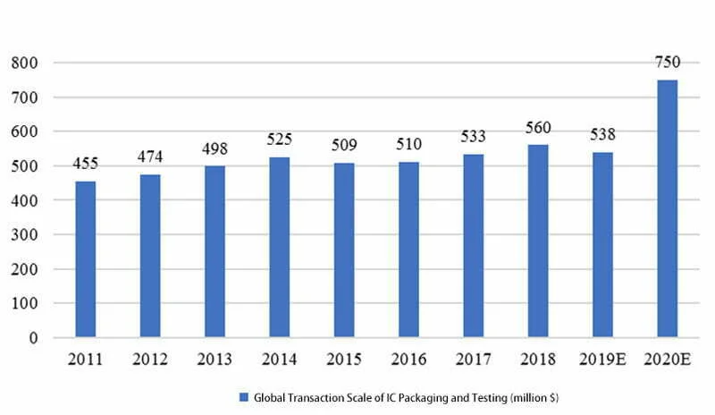
1.1 Global IC Packaging and Testing transaction (2011-2020)
In 2019, the overall semiconductor industry slowed down and showed negative growth, as well as the chip packaging and testing market. However, the later market recovered because the demand for 5G, AI, IoT, cloud computing and big data. Experts predicted that the overall chip packaging and testing market in 2024 can reach $75 billion.
1.2 Global Output of IC Wafer (2012-2022)
With the acceleration of emerging fields such as 5G, IoT, and AI, the required size of chips is getting smaller and smaller. At the same time, there are more and more types of chips. The number of I/O pins has also increased significantly, and the demand for advanced packaging has gradually increased.

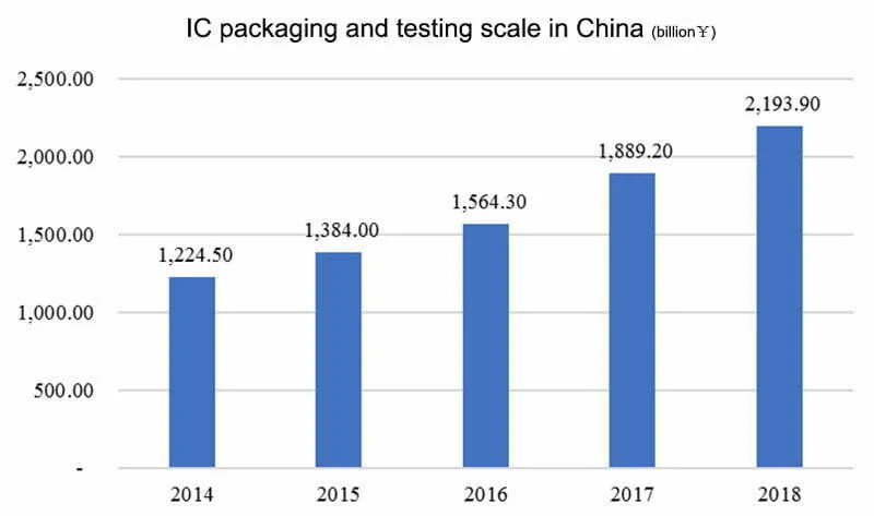
1.3 iC Packaging and testing scale in China (2014-2018)
In 2018, the IC packaging and testing capacity in mainland China reached 217.44 billion pieces, and the market size of the IC packaging and testing industry reached 219.39 billion yuan, a year-on-year increase of 16.1%.
2. The growth of advanced packaging scale
2.1 Proportion of Advanced IC Packaging in total
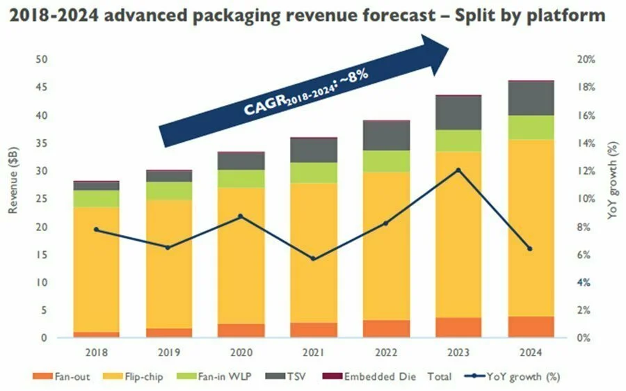
According to Yole statistics, although the overall semiconductor industry slowed down and experienced negative growth in 2019, the advanced packaging market size will maintain a growth trend. In 2018, the advanced packaging market size was US$27.6 billion.
Growing at a compound annual growth rate of 8%, reaching approximately $44 billion by 2024. The traditional packaging market will grow at a compound annual growth rate of 2.4%, while the CAGR of the entire IC packaging industry will reach 5%.
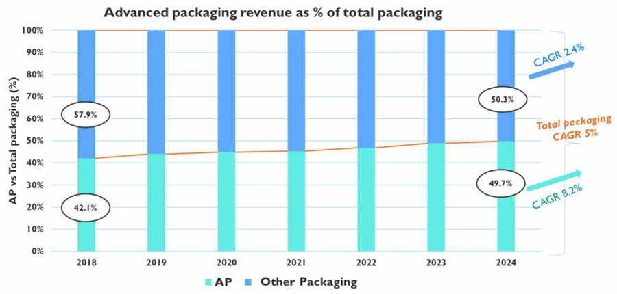
2.2 Advanced Packaging revenue forecast trends (2018-2024)
In the advanced packaging business, flip-chip technology accounts for the highest proportion. In 2018, flip-chip packaging and testing revenue accounted for about 81% of the advanced packaging market. By 2024, due to the rapid development of other technologies, it will drop to 72%.
From 2018 to 2024, TVS, ED and fan-out are the fastest growing technologies . The revenue growth rate of 2.5D/3D packaging (TSV), ED and fan-out packaging (Fan-out) is forecast to be respectively 26%, 49%, 26%.
The CAGR of Fan-in WLP 2018-2024 is relatively low, only 6.5%, and the market size of embedded die in 2018 is less than US$25 million.
However, the CAGR will be as high as 49% in the next five years, and the main driving factors will come from the demand of communication facilities, automotive electronics and mobile markets.
2.3 advanced packaging applications
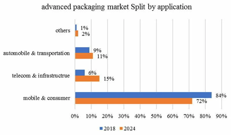
By application field, in 2018, mobile and consumer applications accounted for 84% of the total advanced packaging market. From 2019 to 2024, the CAGR of this segment of the application market was 5%, and in 2024, it accounted for 72% of the total advanced packaging market.
The telecom and infrastructure segment is the fastest-growing segment of the advanced packaging market (about 28%), and its market share will grow from 6% in 2018 to 15% in 2024.
At the same time, the market share of the automotive and transportation segment growed from 9% in 2018 to 11% in 2024.
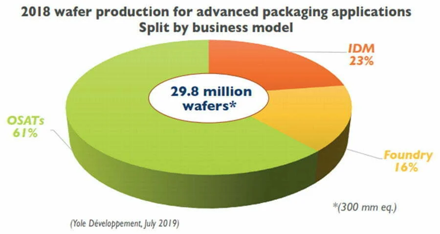
In 2018, professional chip packaging and testing foundries accounted for 61% of the advanced packaging and testing market, while IDM-type companies accounted for 23% and foundry-type manufacturers accounted for 16%.
Competitive Landscape
1. Top 10 global companies (2018-2019)
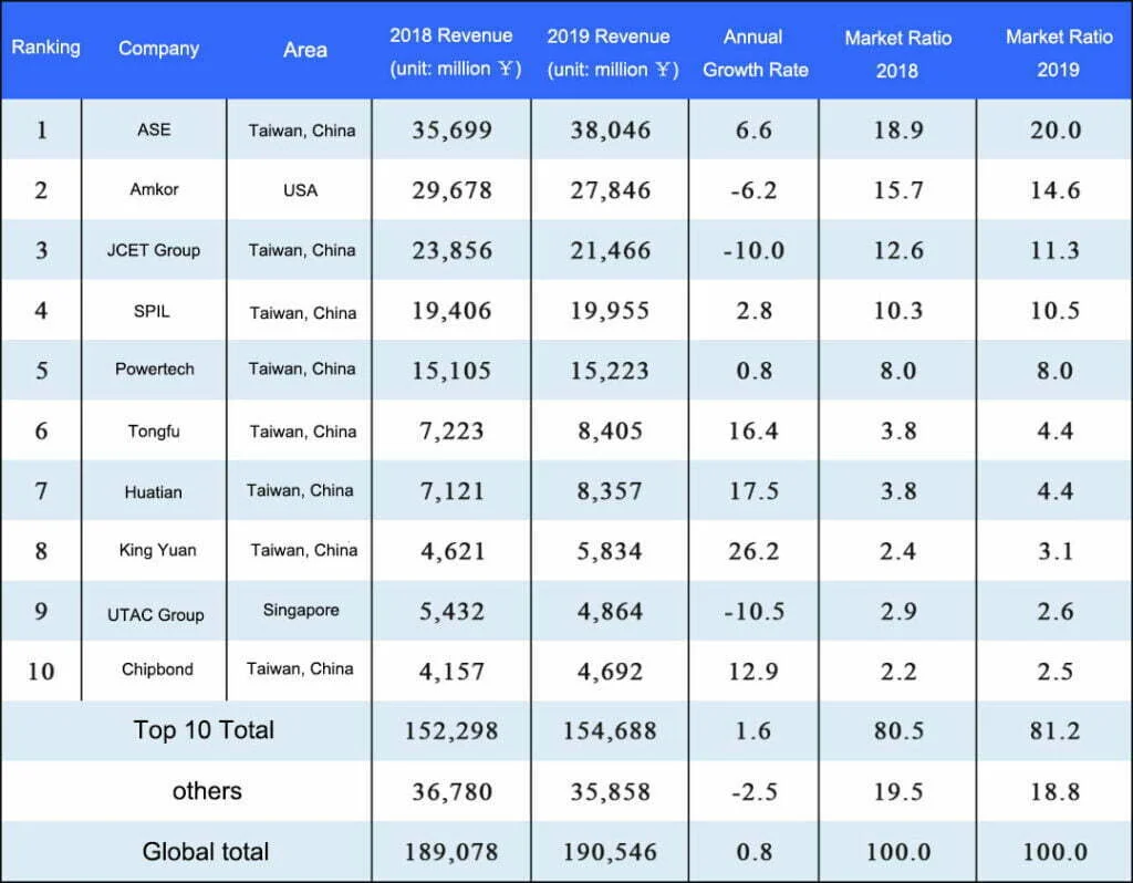
The chip packaging and testing market is relatively concentrated. The top ten manufacturers control about 80% of the market. Manufacturers from mainland China and Taiwan dominate the market. For many years, the Taiwanese packaging and testing industry has captured nearly half of the world’s operating revenue, firmly establishing himself among the top ten.
Regardless of the chip packaging and testing revenue of IDMs (such as Intel and Samsung), ASE and Amkor are firmly in the top two in professional chip packaging and testing.
2. Opportunities and Challenges
Changes in the semiconductor supply chain, shifts in business models, and uncertainty in the U.S.-China trade relationship have created opportunities for some manufacturers and threats to others.
2.1 Extension of industrial chain
In this ever-changing business environment, the semiconductor supply chain is changing at every level. Some vendors have successfully extended new business models.
Significantly affected the IC manufacturing chain, while other manufacturers failed to take advantage of the momentum. Different vendors have different drivers driving them to expand into new businesses.
For example, software companies such as Google, Microsoft, Facebook, and Alibaba are designing their own processors to gain system-level integration/customization and supply chain control at the assembly level.
The biggest change is foundries starting to expand into the advanced packaging business . Although they are relatively “newcomers”, their impact is huge.
2.2 Packaging technology innovation
TSMC leads innovation in fan-out packaging and 3D advanced packaging platforms. They offer a variety of products such as InFO (and its variants), CoWoS, WoW, 3D SoIC, and more.
Advanced packaging has become a mature business for TSMC. They expects it’ll generates $3 billion revenue in 2019, that would place it fourth in the OSAT rankings.
UMC is a major supplier of silicon interposers for 2.5D packaging. They have recently partnered with Xperi to optimize and commercialize ZiBond and DBI technologies for various semiconductor devices.
Meanwhile, Wuhan Xinxin (XMC) provides 3D IC TSV packages for image sensors and high-performance applications. Collectively, these players have played a major role in moving packaging from substrates to silicon platforms.
2.3 System level packaging tends to be popular
It is a trend that participants in the SiP packaging industry chain extend upstream and downstream. In the traditional SiP packaging industry chain, the representative companies of IC packaging and testing include Changdian Technology and ASE , which mainly provide functional-level standard packaging and testing products. The representative company of system-level packaging is USI, which mainly does module-level system packaging. These two companies belong to the upstream and downstream relationship, and their processes and equipment involved are different.
2.4 Embedded Chips
On the other hand, IC substrate and PCB manufacturers such as Samsung Electro-Mechanics (SEMCO), Unimicron, AT&S, and Shinko Electric (Shinko) are taking advantage of embedded chips (and passives) in panel-level fan-out packages and organic substrates. components) into the advanced packaging space and are eating into OSAT’s market share (especially in the business involving advanced packaging).
3. Advanced Packaging Wafer Market Share
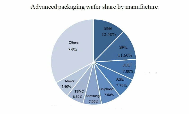
Compared with the overall packaging and testing market concentration, the advanced packaging and testing market concentration is relatively low. In 2017, the top 8 manufacturers accounted for 67% of the advanced packaging market share.
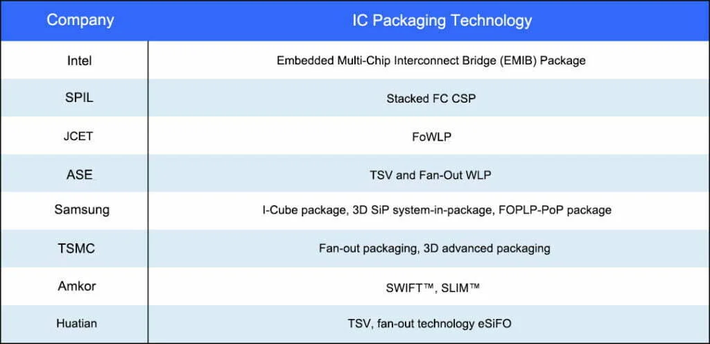
Vendors in the advanced packaging market have different areas of expertise:
Situation of China IC Packaging Industry
Chinese’s IC packaging industry started very early and developed rapidly, it is mainly based on traditional packaging products. In recent years, domestic manufacturers have passed mergers and acquisitions. At present, the Chinese’s technology platform has basically synchronized with overseas manufacturers. Further more, the advanced packaging technologies such as BGA, TVS, WLCSP, and SiP have been mass-produced.
However, there is still a certain gap between the overall revenue of advanced packaging in Taiwan and the United States. According to the statistics of TrendForce, China’s advanced packaging revenue in 2018 was about 52.6 billion yuan. It accounted for 25% of the total domestic packaging and testing revenue, lower than the global ratio of 41%. So there is still much room for growth in the future.
China Advanced IC Packaging Market
In addition, there is also a big gap between mainland packaging companies and international leading manufacturers. Especially, the gap is obvious in high-density integrated circuit packaging technology, such as HPC chip packaging technology. The SoC multi-chip 3D stacking technology proposed by TSMC. It adopts a non-bump bonding structure, which can greatly improve the overall computing speed of CPU/GPU and memory. Intel also proposed a similar 3D packaging concept, stacking memory on CPU and GPU chips.
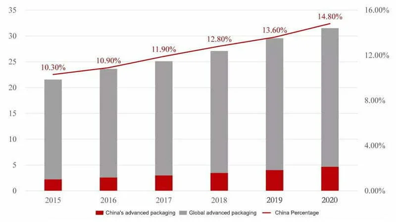
The global output value of China’s advanced packaging market is relatively low, but it is growing rapidly and its proportion is expanding. Yole data display. In 2017, China’s advanced packaging production value was US$2.9 billion, accounting for 11.9% of the world, and it will reach US$4.6 billion by 2020, accounting for 14.8% of the world. According to the data, Chinese packaging and testing companies accelerated the increase in production capacity in the field of advanced packaging in 2018, with a growth rate of 16%, twice the global rate.
market driving force
There are two development paths for advanced packaging:
One is to reduce the size to make it close to the chip size. An important indicator is the ratio of chip area to package area. The closer this ratio is to 1, the better, including WLCSP, FC, Bumping, Fanout, etc.
The second is functional development, which emphasizes heterogeneous integration and provides multi-functionality in system miniaturization, including TSV, SIP and so on.
1. SIP Technology
The global semiconductor manufacturing process is approaching the physical limit of diodes. The most advanced process is 7nm. Due to the huge investment, it becomes more and more expensive to further improve the chip performance from the manufacturing side. Starting from the chip packaging, the system-in-package technology SIP combines chips with different functions such as logic chips and memory.
Passive components IPD, RF RF and sensors and other chips are packaged in one module, which can reduce the chip size, improve chip performance and reduce power consumption. The Internet of Things (IoT) is an important application scenario that promotes the development of SIP packaging technology, and wearable devices are a field with great application potential for system-in-package technology in the future. The fingerprint recognition sensor, 3D face recognition sensor, WiFi wireless network and other functional modules in Apple Watch are packaged together, which is the use of ASE’s system-in-package (SiP) module technology.
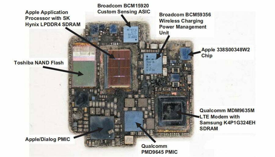
SIP technology successfully integrates integrated circuits, discrete devices, optical devices, memories, multilayer ceramic capacitors, and chip resistors into thin, thin and short substrates without their information interfering with each other. We believe that Apple is at least ahead in the application of system packaging Competitors for one to two years. According to different application requirements and product complexity, the types of system-in-package SiP can be divided into 2D modules containing multiple active and passive components and more complex 3D modules. For example, PiP (Package-in-Package) in the system, PoP (Package-on-Package) and 2.5D/3D packaging technology on the system.
2. TSV Technology
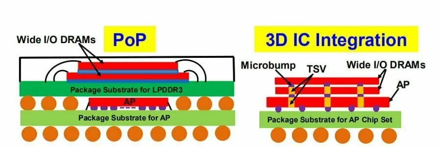
As a representative of 3D packaging technology, TSV technology will have greater applications in the field of 3DNANDFLASH flash memory packaging and DRAM memory packaging in the future. Memory has become the sub-section with the most growth potential in the domestic semiconductor field. The two major memory projects, Yangtze Memory (NAND FLASH) and Hefei Changxin (DRAM), will be mass-produced in 2020, which will undoubtedly be huge for domestic manufacturers with advanced packaging technology. growth opportunities.
3. Fan-out
Entering the 5G era, in order to obtain higher data transmission rate and bandwidth capacity, higher frequency electromagnetic waves must be used as the transmission medium, and the wavelengths are shorter and enter the millimeter wave level. The two mainstream frequencies in the 5G era, the Sub-6GHz frequency band and the 28GHz millimeter wave frequency band, due to the increase of the frequency, the result of the wavelength drop is that the antenna is shorter, so the antenna is expected to be integrated into the chip in the 5G chip era to simplify the design and Can reduce costs.
There are two possible packaging technologies for next-generation 5G chips: AiP (Antenna in Package) with a substrate and a fan-out package without a carrier board. Since the second fan-out packaging scheme does not require a substrate, it can further reduce costs and reduce the chip size on the basis of integrating multiple chips, so the fan-out packaging technology maybe become the mainstream technology of 5G chip packaging.
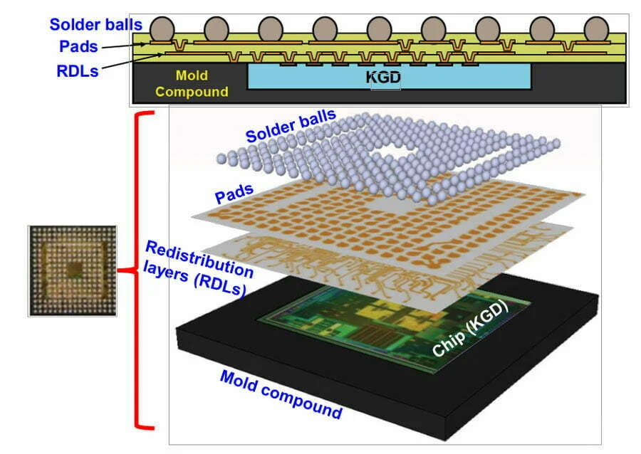
Each electronic module in the car adopts different packaging technologies, and the packaging of the millimeter-wave radar chip in the automotive electronics will also use a large number of Fan-out packaging technology.
The domestic packaging and testing factory Changdian Technology acquired eWLB packaging technology after acquiring Xingke Jinpeng, becoming one of the early packaging and testing manufacturers in the field of millimeter-wave radar. Huatian Technology is expected to make efforts in this field after recent technological breakthroughs.
Technology development direction
There are two types of semiconductor packaging: traditional packaging and advanced packaging. With the continuous expansion of the scale of advanced packaging, the proportion has gradually approached and surpassed the trend of traditional packaging. For the semiconductor industry, packaging and testing is no longer just a separate foundry link in the past, but an integrated solution that combines design, material and equipment.
Therefore, advanced packaging is becoming more and more important in the field of semiconductor packaging and testing. According to Yole’s forecast, the global advanced packaging market will reach 44% of the overall integrated circuit packaging services by 2020, with an annual operating income of approximately US$31.5 billion; China’s advanced packaging market will reach US$4.6 billion in 2020, with a compound annual growth rate of 16%. From a technical point of view, FOWLP, SiP, and 3DTSV are the three most concerned advanced packaging and testing technologies.
1. FOWLP Packaging
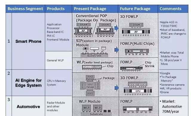
FOWLP package refers to a new method of combining multiple dies from heterogeneous processes into a compact package. It was first proposed by Intel. The advantages of FOWLP over fan-in packaging technology are: reduced package thickness, scalability (for increasing the number of I/Os), improved electrical performance, good thermal performance, and a substrateless process.
2. SiP Packaging
System-in-package (SiP) is a new type of packaging technology at the highest end in the field of IC packaging, which integrates one or more IC chips and passive components in one package. SiP is an ideal solution that combines the advantages of existing core resources and semiconductor production processes to reduce costs and shorten time to market. At the same time, it overcomes difficulties such as process compatibility, signal mixing, noise interference, and electromagnetic interference in SOC. Moreover, the application of SiP is very extensive. At present, the output value of smartphones accounts for the highest proportion, about 70%.
The increasing demand for SiP packaging brought about by the commercial use of 5G technology. First, due to the increase in the value of stand-alone RF, the overall market size of RF front-end has grown rapidly. There is a general trend toward modularizing RF front-end, 5G millimeter-wave antenna, and RF integration components, which are usually based on GaAs. The 5G antenna is primarily composed of LCP (Liquid Crystal Polymer), and SiP packaging is well suited for heterogeneous integration. SiP packaging is expected to become more popular in the RF sector.
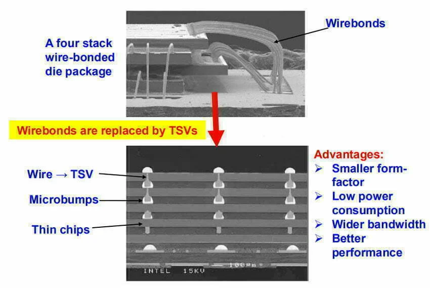
3. 3D Packaging - TSV
3D packaging improves core performance such as size, weight, speed, yield and energy consumption, and is considered by most semiconductor manufacturers as the most promising packaging method. As the tentacles of advanced packaging continue to extend to advanced technologies with high performance and high-density integration, TSV, known as the fourth-generation 3D packaging technology, is expected to become a sustainable driving force for the future development of advanced packaging.
