
The Half-Bridge Topology
The half-bridge topology as applied to a DC-DC converter uses two transistors to initiate switching action, which will deliver current pulses to a load. Alongside rectification and smoothing with a capacitor bank, this DC-DC converter topology provides pulses that can be smoothed to a nominal DC power value. This topology can be isolated, where output power is coupled through a transformer or optocoupler. Isolation might be implemented inside the gate driver circuit (if present as an IC), which might be done through junction isolation. Non-isolated topologies might also use transformer coupling to step up or down the output voltage, but these are run at lower output currents for safety purposes.
Example Half-Bridge DC-DC Converters
The graphic below shows some examples of half-bridge DC-DC converter implementation; the right circuit uses an optocoupler to bring the driver signal to the output side. The left circuit could use an optocoupler built into the chip, or a small transformer with the drive circuit on the secondary side. Either of these topologies could be isolated simply by splitting grounds across the coupling element. The coupling element could also be removed entirely if it is not required, although this would normally only be appropriate at lower voltages/currents and slower switching edge rates.
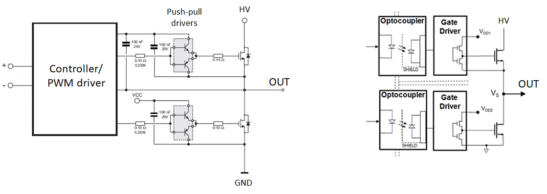
Two example drive stages in a half-bridge DC-DC converter.
Note that the driver stage could be coupled with an optoisolator working at logic levels; this requires a high power source on the output side to provide high power delivery and might be used in motor control. Transformer coupling allows for high voltage or high current output, thus power would be coupled to the output rather than the driver signal. In this case, the driver circuit would be on the primary side of the transformer, and there would be ground plane split across the transformer due to the need for isolation and user safety.
Driver and Feedback Stages
For lower current systems, it’s possible to find an IC that implements the isolation and driving functions into one component. At low currents of about a few Amps or less, these might also include the FET stage that drives power to a filtering/smoothing circuit on the output. These components are normally isolated internally with an optocoupler as this keeps the footprint very small; external components required may include diodes, a capacitor bank, and inducto, all of which help reduce ripple on the output.
Higher current systems will always use a driver circuit, as indicated in the above graphic. There are many highly integrated components that include a feedback sense input, which will be used in an internal control loop to compensate for variations in the output power. Depending on the output current value, a current-sense amplifier might be used to read the output power and provide a scaled output to the driver’s feedback sense pin. The driver can then automatically adjust the PWM signal to maintain regulation. Normally the duty cycle is adjusted in this application. If a totally custom control method is to be used, it may need to be implemented in an MCU or small FPGA, which would then control the frequency and/or duty cycle of a PWM driver or oscillator circuit.
Finally, there is often a question of what type of transistors to use in the driver stage, particularly given the availability of advanced materials like SiC and GaN. The answer depends on the voltages being supplied by the driver stage. The output voltage from these systems can be quite large when the FETs are placed directly in the output current loop, especially in transformer coupled systems that step up the required voltage. These more advanced materials provide other benefits in terms of heat dissipation and thermal management. The table below summarizes when different semiconductors should be used based on their Vgs values and their voltage ratings. Note that some of these can be switched deeply into the ON state at logic levels.

Mains Input Example
The image below shows an example half-bridge DC-DC converter block diagram for a system with standard mains inputs (85-265 V AC). This system uses isolation for safety purposes from AC and rectified DC power, and it steps down voltage from the rectified high DC voltage to the moderate output voltage level. This type of design could be used to produce standard voltage levels (e.g., 24 V DC, 48 V DC). This type of system would be used in, for example, server power supplies, appliances, and industrial power supplies.

The half-bridge drive circuit with feedback is shown below. This is just an expansion of the standard half-bridge driver topology shown above, but with a feedback loop implemented with a current-sense amplifier (CSA), optocoupler, and the Sense input on the PWM generator. The transformer could step up or step down the voltage depending on the load requirements, and the inductor and capacitor (L-circuit) perform the same function as in a standard DC-DC converters operating at lower currents. The example below implements buck conversion in voltage mode.
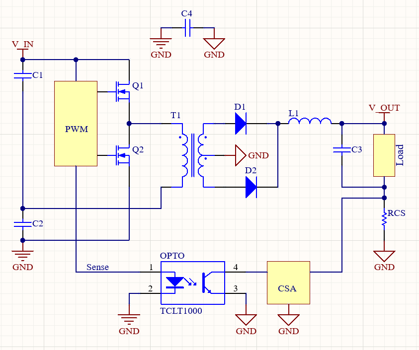
DC-DC conversion and regulation section. This could be used as the regulator section in a power supply that receives mains input power in the block diagram shown above.
Half-Bridge DC-DC Converter PCB Layout
Before approaching the layout, make sure you’ve planned the stackup appropriately. This involves the following design considerations:
- Material selection: Make sure to select appropriate materials that can operate appropriately at the voltages being implemented in your half-bridge DC-DC converter. Typically, these will be high-CTI substrate materials when high voltages are involved. There is also a need for high-Tg when the converter will operate at high current and/or high temperature.
- PCB stackup: As we’ll see below, keeping low-inductance and preventing excess parasitiic capacitance will depend on location of ground with respect to power rails in the system. The loop inductance in specific nodes in the circuit can be controlled with nearby ground. As such, a 4-layer board with ground planes is the best starting point for stackup design.
Following these points, you can plan the PCB layout for your half-bridge DC-DC converter design. Each stage of the PCB layout should be laid out and routed much like any other power supply layout to help reduce noise. In the case where the half-bridge DC-DC converter design needs to be isolated, ground plane regions must be used in the layer adjacent to components and signals; only split the plane regions across the gaps defined by the optocoupler/transformer elements in the PCB layout. A schematic example with transformer coupling in a PCB is shown below.

Rough strategy to try and layout a half-bridge DC-DC converter.
A note on the capacitor bridging the ground regions: make sure this is a safety capacitor (usually Y-type) that offers higher capacitance than the transformer interwinding capacitance; this ensure EMI (ESD events) move through the capacitor and not across the transformer gap. Also note the leakage current; this could be on the order of mA and could create an annoying shock if the user interacts with the ground terminal on the output side. This would actually unacceptable in medical equipment; those systems would require lower leakage over higher capacitance.
Regarding routing in high power output systems, rails are normally used on the output side to route into a connector. This assumes the converter is being designed as a standalone module, something which we’ve done for server power supplies. The routing on the output power rails could also go directly to a load implemented on the same board, which we’ve done for a high power motor controller. Whether output routing is placed as rails or with a power plane depends on the current output from the design. In my opinion, rails are preferred with a row of vias on the low side of the load to connect back to the secondary/output side ground plane.
Noise in the system is its own beast, but using a ground plane adjacent to the main component/signal layer will go a long way to help reduce radiated emissions and coupling. Conducted EMI filtering (common-mde) is most effective on the input side as this helps suppress common-mode loops coupled capacitively through the device chassis, but these should also be used on the output in high current systems to help prevent common-mode surges. Take a look at some of our other tips on noise reduction in switching converters to learn more.