What is a Coplanar Waveguide Calculator?
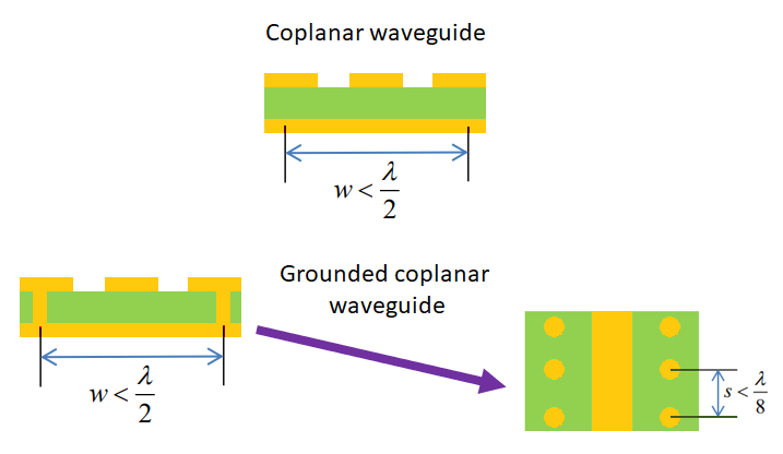
A coplanar waveguide is a simple routing style where a trace is routed on the surface layer and surrounded by ground pour on each side. In addition, routing is done above a ground plane, providing high isolation in the PCB layout. In addition, a via fence can be used to tie the ground pour back to the ground plane for even higher isolation, known as grounded coplanar waveguide routing. Both varieties are shown below.

Coplanar waveguide design
When you need to implement impedance control in your PCB, you’ll need to determine the PCB trace width that best suits your design and ensures your trace impedance takes the correct value. This is where a coplanar waveguide calculator becomes important. The designer can normally enter their desired impedance, and the calculator will determine the PCB trace width needed to meet that impedance goal.
Factors Affecting Coplanar Waveguide Impedance
When calculating coplanar waveguide impedance, there are many factors that affect the waveguide’s impedance, losses, and isolation:
- Geometry: The width of the central trace and the spacing between the trace and ground pour will determine the field distribution around the trace, which then determines how much loss signals experience and the level of isolation provided by the surface ground pour.
- Substrate dielectric constant: The dielectric constant of the substrate has dispersion, which will determine the amount of loss seen at different frequencies. Dispersion also determines how different frequencies travel at different speeds.
- Copper roughness: At high frequencies (microwave and mmWave), copper roughness will increase the impedance of an interconnect. Most online calculators do not account for copper roughness.
- Skin effect: The skin effect in a PCB trace, including coplanar waveguides, adds additional AC and DC resistance to the total impedance.
The best coplanar waveguide calculator can account for all of these effects simultaneously and without a complex 3D field solver. The best PCB stackup design and routing tools will include these calculations to help designers ensure impedance control throughout the required bandwidth for their signals.

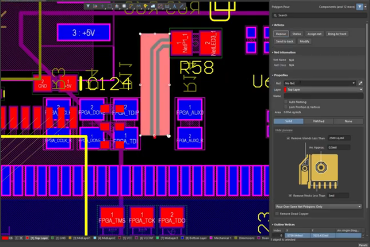
Designing coplanar waveguide geometries is easy with the powerful routing tools in Altium Designer.
Using a Coplanar Waveguide Calculator
A coplanar waveguide calculator will operate in one of two ways. Either the desired impedance at a specific frequency is used to determine the waveguide width, or the width is entered and the impedance is calculated. In both cases, you’ll need to enter your stackup information into the calculator to get accurate results. These calculators will also return the effective dielectric constant seen by signals propagating on the waveguide.
The problem with online coplanar waveguide calculators is that they do not include dispersion, copper roughness, skin effect, or loss tangent in the PCB substrate. The major problem with neglecting dispersion is that the impedance calculated at one frequency may no longer be correct at any other frequency. Therefore, these calculators are only useful for a single frequency and cannot treat broadband signals in real PCBs. This is why designers need an advanced coplanar waveguide calculator for high-frequency PCBs.
Advanced Coplanar Waveguide Calculator Functions
More advanced coplanar waveguide calculator utilities will include all the effects mentioned above when calculating the impedance and effective dielectric constant of the waveguide. In addition, they can consider the dielectric constant of the PCB substrate throughout your signal’s bandwidth. This gives you an ultra-accurate impedance and width calculation, which can then be used in your PCB layout and routing tools.
