Design Principles and Ideas
The physical characteristics of flash memory are fundamentally different from those of common memory: currently, all kinds of DDR, SDRAM, or RDRAM belong to volatile memory, and the data in the memory cannot be retained as long as the current supply is stopped; flash memory can retain data for a long time without current supply, and its storage characteristics are equivalent to that of a hard disk, which is the basis for flash memory to become the storage medium of various portable digital devices.
This design uses a W25Q128FV 128M flash memory chip, and you can download the device manual on the official website. Here, for your convenience, we also provide it to you. If you need to use it, you can reply "W25Q128FV manual data" in the WeChat official account, and you can design it flexibly according to the actual project application.
The storage of this flash chip is 4KB per sector, 256 words can be stored in one sector, one word is 8 bits, one block is 64KB, and a total of 256 blocks form a storage flash memory.
In the following explanation, we will mainly talk about the implementation of byte read and write. The protocol used in this design is the SPI protocol, and this chip supports QSPI, dual-port SPI, etc. Flash has three status registers, and each bit of each status register has its own function. You can specifically look at the device manual. First, let me briefly explain the first status register.
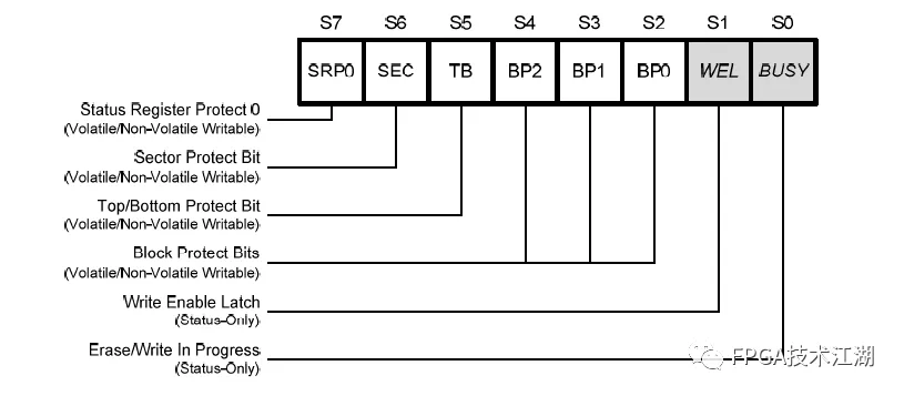
The first bit of this status register is a readable, busy, and not busy flag. You can determine whether the chip is busy or not in our design to determine whether to proceed to the next step. The second bit is a write flag signal, which is 1 when the write enable is turned on, and only when it is 1 can we perform writing. It is worth noting that this flag will become 0 after either a page operation or an erase command. Then the previous commands can be regarded as protection commands, with specific logical functions for use.
In flash, before writing data, you must first erase the data (where you want to erase), and then write. If you have not used the flash chip, then you can not erase it because the flash does not lose data when powered off.
The design idea is大概 to first read out the device manufacturer and chip ID, then write the command, turn on the write enable, perform a page operation to write data (it is worth noting that our FLASH is new, so no erase command is performed. It is recommended to erase --- turn off the write enable -- turn on the write enable), then read the first register to determine whether the first bit of the chip is busy, and if not, perform a read operation and then display the data we wrote on the digital tube.
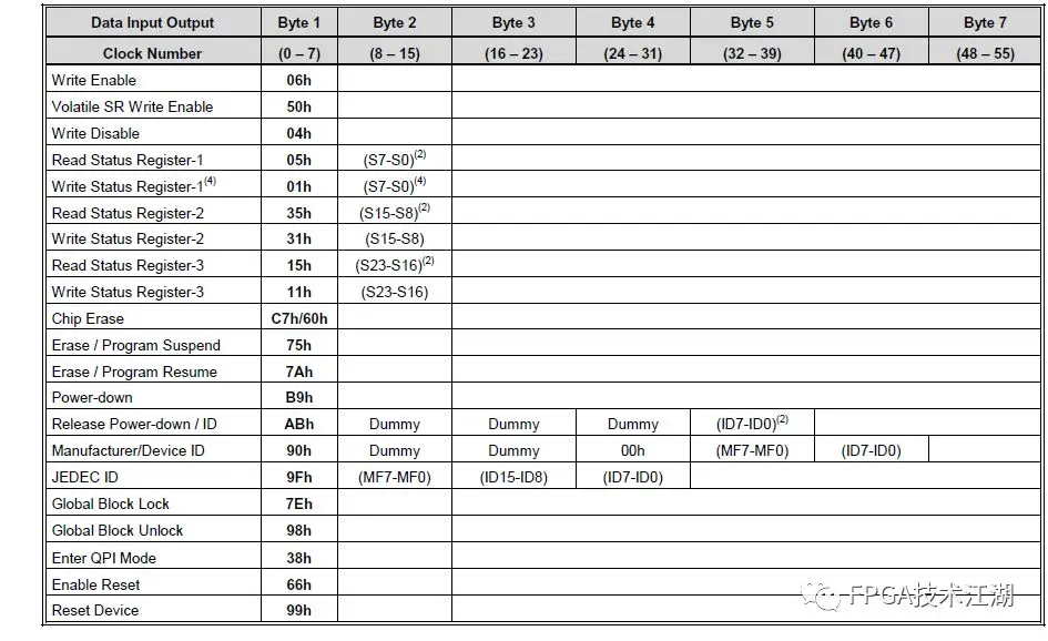
Some operation commands are as follows:
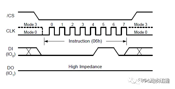
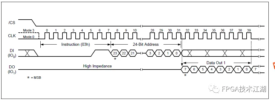
Our transmission format is to write the command on the rising edge of the clock and read the command on the falling edge of the clock, using the standard SPI protocol. Ports IO0 and IO1 are both unidirectional.
Write enable timing:
Read enable sequence:
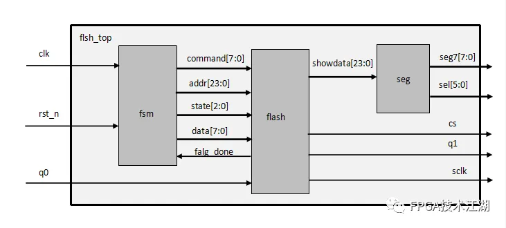
Design framework
In this design, an FSM controller is used to control what commands are sent. The flash module determines the state signal sent by the FSM to select what operations should be executed. When the command is written or read out, the flag_done command is sent to let us judge whether the previous command is completed. FAM will send the next command if completed. The overall architecture diagram is as follows:
Design code
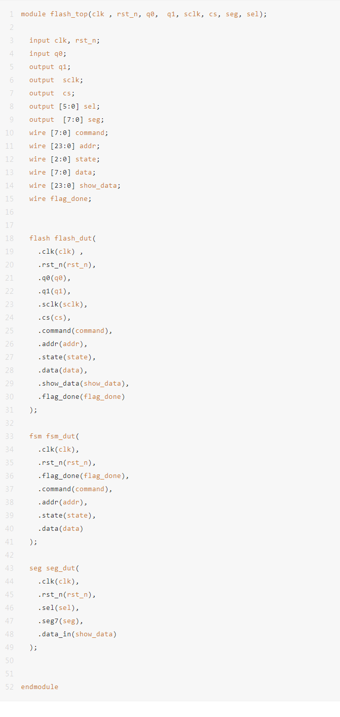
Top module flash_top code:
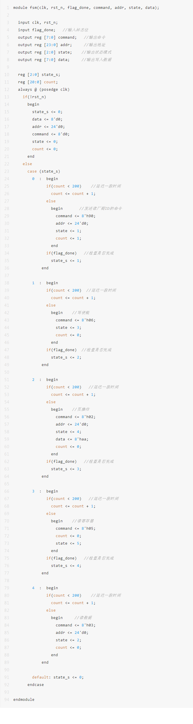
Design module fsm code:
Intermediate module flash code:

Nixie module seg code:
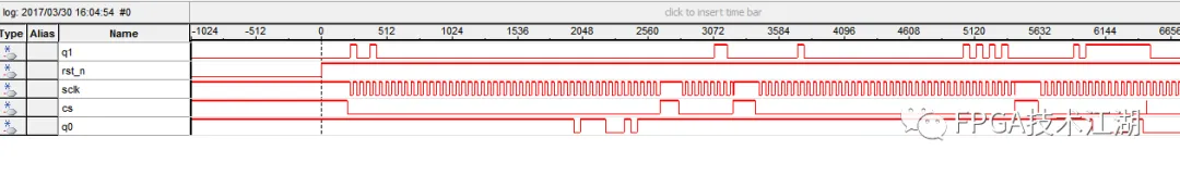
SignalTap Collection diagram