Impedance control is an integral aspect of everything related to PCBs. It is necessary for all stages – starting from design to implementation. Overlooking impedance control can be disastrous for PCB designers and engineers alike.
You may buy PCBs from different sources or order custom high-speed PCBs. However, neglecting impedance control may result in complete non-functional PCBs
The article introduces nine tips to secure impedance control in your PCB Design.
Understand the Basic Factors of Impedance Control
Connecting wires in the PCBs perform more than one function. Besides current flow, they also have a part in the signal transmission lines. The multi-functionality helps in maximizing output from small sizes and digitalization.
It is crucial to prevent the reflection of signal transmission in PCBs. Impedance Control, aligning, and matching the impedance can reduce Transmission loss in circuits. Impedance is a characteristic trait among AC circuits. It is the resistance parallel loops and power planes offer to the flow of AC.
A variety of reasons can affect the characteristic impedance of your PCB design. Many errors arise from faulty transmission lines.
Characteristic impedance may also vary due to other causes. Possible factors include:
1. Circuit trace thickness.
2. Prepreg around the circuit trace Dielectric values.
3. Insulator thickness also plays a part.
Choose the Right Dielectrics
Dielectric constant can affect the characteristic impedance in a big way. It is necessary to calculate the amount of controlled impedance of your PCB Design. The characteristic impedance is proportional to the width of the dielectric material. Larger the width of the insulating dielectric, the higher the impedance value.
Manufacturers use Dielectrics in PCB Circuits for insulating purposes. An ingredient in substrate boards- choose from a large number of component materials. The popular ones include FR-4- a fiberglass-epoxy laminate. It is flame-resistant as well- a useful property in case the PCBs get overheated. Based on your design- you can also choose flexible FLEX materials.
The dielectric constant is variable about frequency. Choose materials having a consistent, constant value through a wide range of frequencies. They are suitable for high-frequency applications of your PCB board.
Prevent Crossing Traces across Split Planes
Experts suggest routing the high-speed/frequency signals over a ground reference plane. Look to avoid routing trace wiring across split planes at all times. The only time of exception is if you want to increase the controlled impedance.
There are several negative aspects of crossing traces across split planes. Some of them include:
1. Signal transmission delay due to series inductance.
2. Signal disruption and interference.
3. A decrease in signal integrity.
An alternative to cross-tracing is the use of stitching capacitors across split planes. They provide a proper return path for the current. It leads to a reduction in the current loop area. This way, you can have the desired impedance control.
Always Keep A Reference Ground Plane
We need to refer to the ground path as a return path for alternating current. Most of the area not occupied by circuit traces make up the reference ground plane. The large area permits return of large currents without a significant voltage drop. For PCBs operating on Radiofrequency levels, the ground plane reduces signal disturbances. It also decreases interference through ground loops.
The ground plane is also essential for impedance control. Further, it prevents crosstalk between 2 side-by-side circuit traces. It also prevents significant voltage drop during the circuit’s change of state. Power supplies or ground traces with high impedance can cause a ground bounce.
It disrupts the functions of other circuit components. The large area of the reference ground has less impedance. As a result, the current pulses cause less damage.
Know about the Pre-preg Limitations
The prepreg (short for pre-impregnated) finds its uses in fusing etched cores. Its other application- attaching a copper wire to the base. The reinforcing component may have several constituent materials. In general, it usually consists of fiberglass and an epoxy-based resin material. Pressing the two layers at high temperatures creates the required thickness.
Experts recommend using at most three different types of prepreg during a core stack-up. Each layer should be less than 10 millimeters to avoid thickness variation.
Avoid prepregs having low resin content. They may lead to resin starvation during the time of lamination. The boards should be symmetrical in design. For greater impedance control, dielectric constant uniformity is necessary. Greater consistency is also desirable.
Besides, dielectric constants in prepreg fused materials vary. They usually differ compared to the original core materials. Opt for prepreg materials comparable to Copper’s CTE (Coefficient of Thermal Expansion).
Impedance Control Traces Size
Traces are useful in determining the controlled impedance of your high-speed PCB Board. Calculate the impedance control using the trace dimensions. The four measurements needed for this calculation are:
● H: Height of the trace.
● Er: Dielectric Value.
● T: Thickness of the evidence.
● W: Width of the evidence.
Use a Secure Impedance Calculator
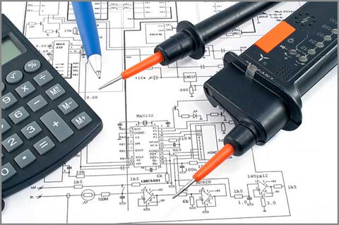
Calculating the level of impedance is crucial in several stages. It is particularly necessary during the PCB Design Stage. Find the value of the controlled impedance in your PCB Design. Afterward, you can decide on changes or the accepted level of tolerance.
The main problem is the calculation itself. The impedance value equation involves a series of tiring complex equations. Other than dimensions, you would also be needing the values of dielectric constants. You would need to know accurate logarithmic values, values of functions, and many more. It is also not possible to have a scientific calculator nearby at all times.
Online options for calculating impedance are available nowadays. Several sites do the calculation part for you. Present the trace dimensions and the value of the dielectric constant. You will have the impedance value in no time.
A Good PCB Design Tool is Essential
With technological progress, a lot of helping options are now available. Tools and software for PCB design were unheard of a few decades ago. Some even have integrated components for material cost estimates. Try out among the several options available and pick a favorite.
PCB designers try their favorite among Altium Designer, PowerPCB, ORCAD, Autodesk Eagle. Other options include KiCAD EDA, Solidworks PCB, and many more. Each has a few pros and cons. Do consider the compatibility with your current system before purchasing.
Perform A Signal Integrity Analysis
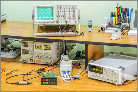
It makes sense to run a Signal Integrity Analysis test before placing your order. The procedure is also logical if you are manufacturing the PCBs yourselves.
Finding out possible errors in the test stage is the right way of cost-saving. It also prevents redundancy, wastage of component materials, trial, and failure. You can find whether the impedance control levels match your desired target. Suggest the manufacturer about the acceptable tolerance levels of the PCB work order.
