An RF PCB design is a bit different from a conventional board. What makes it distinct are parameters like impedance matching, type of traces (preferably co-planar), elimination of via stubs (to avoid reflection), ground planes, vias, and power supply decoupling. Other aspects such as stack-up and material selection also play crucial roles in these boards.
With all these factors in mind, the complexity of an RF design process increases due to elements like EMI interference, high-frequency signal channeling, etc.
Impedance matching
In a controlled impedance RF circuit, maximum power transfer without distortion occurs from source to load when the impedance remains the same throughout the trace. This impedance is known as the characteristic impedance of the trace (Z0). The characteristic impedance depends on the geometry of the traces, such as trace width, the dielectric constant of the PCB material, trace thickness, and height from the reference ground plane. In order to match these impedances, matching circuits are also designed.
Radio-frequency board materials
RF PCBs are manufactured with certain materials that fulfill high-frequency operation requirements. These materials should have low signal losses, be stable over high-frequency operation, and should be able to absorb high amounts of heat. The dielectric constant (DK), loss tangent (tan δ), and coefficient of thermal expansion (CTE) values also require consistency over wide frequency ranges. Typical values of dielectric constant range from 3 to 3.5 for these boards. Loss tangent values are in the range of 0.0022 to 0.0095 for the frequency range of 10-30GHz.
Apart from all these specific necessities, the material cost and ease of manufacturing are also considered.
Materials that are made of Polytetrafluoroethylene (PTFE), ceramics, and hydrocarbons mixed with one another or with a form of glass are commonly used. Rogers material is a common choice for RF circuit boards. There are different variants of Rogers material available. A few of them are listed below:
- RT/duroid
- RO3000
- RO4000
- Rogers TMM
RF PCB stack-up
Radio-frequency board stack-up requires attention to details such as isolation between traces and components, power supply decoupling, number of layers and arrangement, placement of components, etc. A standard 4 layer RF stack-up is shown in the figure below.
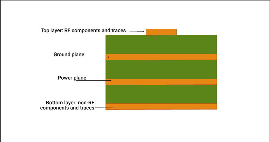
The radio-frequency components and traces are placed on the top layer. This layer is immediately followed by a ground plane and a power plane. All the non-RF components and traces are populated on the bottom layer. This arrangement offers minimum interference between RF and non-RF components. The immediate ground plane provides a minimum path for the ground return current. Thus all-in-all this is a stack-up that is suitable for a small radio-frequency board.
RF trace design
RF traces propagate high-frequency signals and thus are subject to transmission losses and interference issues. The characteristic impedance of these traces is a main concern amongst the designers. In radio-frequency boards, the traces are regarded as transmission lines. The most common types of transmission lines designed are coplanar waveguide (CPWG), microstrip and stripline. Below are the radio frequency trace design aspects that determine proper operation and minimum losses:
- The length of the trace should be as short as possible. This helps to reduce attenuation.
- In the layout, never place an RF trace and a normal trace parallel to each other. If placed like that, interference will occur between the two.
- Ground planes are required to provide return paths for signals.
- The test points are not supposed to be placed on the traces. It will interrupt the impedance matching values of the trace.
- Instead of keeping sharp right turns, gradually curved bends are better for trace performances.
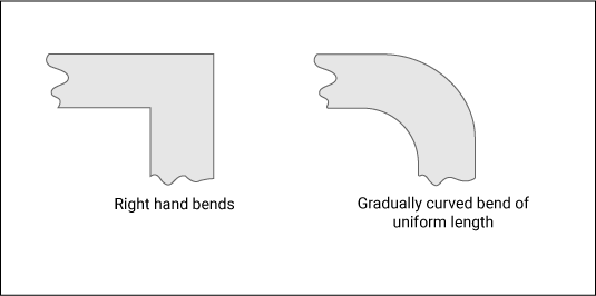
In cases where right-hand bends are unavoidable, a process called metering is used to reduce the ill effects. The metering of a trace is shown below:
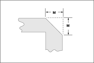
Here, M is given by the following formula:

Design of ground planes
Any radio-frequency trace or component requires a return path for the current propagating through it. A ground plane takes care of this. However, the ground planes need some additional design considerations. Let us have a look at these.
- A dedicated ground plane should be present for each RF layer. This ground plane is placed immediately below the layer to make the current flow path shortest.
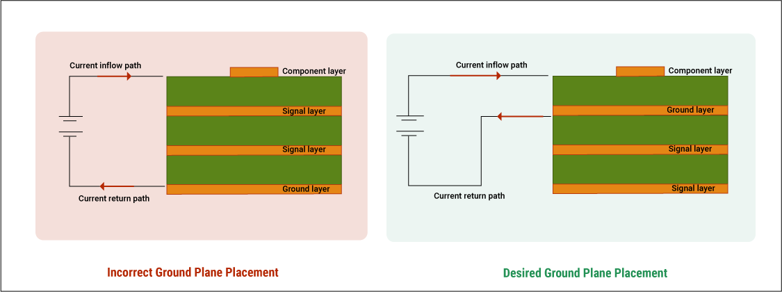
- The ground plane should be continuous. No breaks are allowed. Such breaks might pave way for shorter paths for the current to return.
- For every shunt component placed in an RF transmission line, a minimum of two grounding vias are required.
Via design
Vias in RF traces should be avoided as far as possible. However, if these cannot be avoided, specific via diameters and length must be followed. A via induces parasitic capacitance in a circuit board. In the case of radio-frequency boards, this capacitance affects the high-frequency operation. Therefore, to reduce interference at these frequencies, it is important to design vias keeping in mind the following guidelines:
- In order to reduce the parasitic capacitance, introduce more parallel vias.
- For each of the pins or pads of a component, a dedicated via must be present.
- Implement ground plane via stitching wherever applicable. This establishes a shorter ground return path for the current.
- Reduce routing of RF traces from one layer to another through vias.
- Use the maximum number of vias between the top layer ground plane and inner layer planes as allowed by the design. These vias should be placed at a distance not exceeding 1/20th of the signal wavelength.
Power supply decoupling
Noise reduction is extremely critical when it comes to radio-frequency boards. At the high operating frequencies, these boards become very much sensitive to the effects of noise. Therefore, all possible methods are employed for noise removal. One such method is called power supply decoupling.
Selection of decoupling capacitors
Noise that is carried into the circuit through the power supply is filtered using this process. The capacitors that are designated for this are called decoupling capacitors. These capacitors are connected across the power supply.
Impedance matching is an integral feature of every RF circuit board. Hence after the connection of decoupling capacitors, the impedance of the whole circuit should not change. Stick to the following design considerations to avoid the change in impedance:
- Always connect capacitors with minimum impedance for decoupling.
- Operate the capacitors at the self-resonant frequency (SRF) to yield minimum impedance. SRF value of a capacitor is inversely proportional to its capacitance value.
- Choose capacitors whose SRF is close to the noise frequency.
Placement of decoupling capacitors
The placement of decoupling capacitors is also an important part of getting the RF design right. Given below is a simple circuit that illustrates two decoupling capacitors placed in parallel to an IC component.
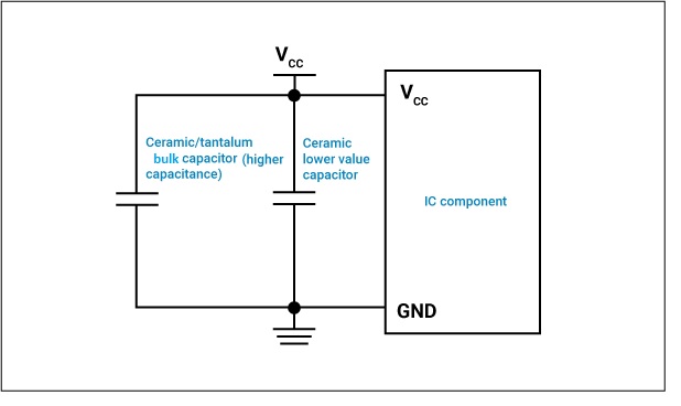
The higher capacitor is meant to filter the low-frequency noise in the system and store the energy. The high-frequency noise is filtered out by the lower capacitor. Other placement related guidelines are:
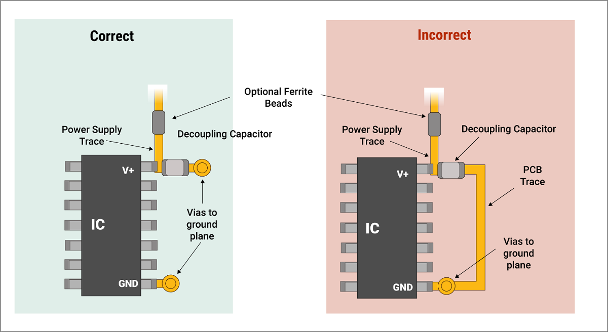
- The decoupling capacitors are to be placed on the same layer as the components.
- Place the capacitors parallel to the signal flow path.
- Keep individual ground vias for each capacitor.
- The capacitors should be placed in ascending order of their capacitance from the supply. That is, the one with the lowest capacitance comes nearest to the power supply.
