
1. IoT PCB design domains
An IoT product typically collects information from the real world, coverts it to the digital one and then transmits data into the cloud. Some analysis likely follows and the results are sent back. As such there are four main IoT design domains:
(a) Analog
(b) Digital
(c) MEMS
(d) RF
Restating the earlier paragraph, a MEMS sensor collects data, it undergoes analog-to-digital conversion for input to a microcontroller and the results are transmitted over standards such as WiFi, Bluetooth and 3G/4G. Depending on the response that is part of the device’s functionality, a backpath digital-to-analog conversion is also likely.
These then are the domains in which the designer will work.
2. IoT PCB form and fit
Wearable devices illustrate the form factor challenges facing many IoT PCB designs. A company developing a smartwatch wants a size and weight equivalent to that of a traditional ‘dumb’ timepiece. IoT innovators generally approach this issue from two starting points:
(a) A potential function is identified and the developers then explore whether it can be fit into an appropriate and marketable shell.
(b) Developer see the chance to add a function to an existing product and then explore whether that can be done with as little impact as possible to the original.
Either way, it is likely that complex functions will need to fit into a tight living space.
3. IoT design components
A major influence on ‘form and fit’ is the proper identification of the components to populate the PCB. Figure 1 shows the example of a Next Thermostat. However, those parts are simply what is required for its operation. Your design might need a fingerprint reader, a different type of MEMS sensor or a different RF standard.
You need to lock these down early – and also, do not forget external interfaces (buttons, switches, charging ports, etc).
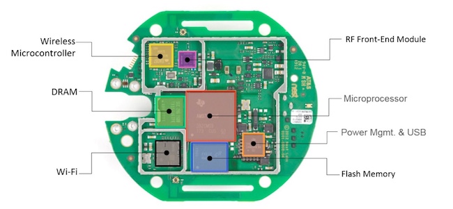
Figure 1. Populating the IoT PCB for a Nest thermostat (Nest)
4. Capturing the IoT PCB design intent in a schematic
You have your component types. Now you must determine how to fit them together, and specify the right part number for the specification and target dollar cost.
Developing a schematic begins to show you how that will happen. Also, the right tools will allow you to conduct analog/mixed-signal circuit analysis and identify some of the possible signal integrity challenges you face before you go to actual layout.
5. Simulation, validation, power and memory in IoT PCB designs.
IoT designs can look simple in function but prove harder to realize than that implies. The old adage applies that you should try to catch as many issues as possible as early in the flow as possible. Consider just these three challenges (there are plenty more):
(a) IoT designs are small and must frequently offer long battery life. They may therefore need to operate across a wide range of power states and perform different tasks (e.g. sensing, standby, Rx/Tx, etc). Each must be functionally verified.
(b) Similarly, what about failure risks due to voltage loss on critical nets? Could some areas on the board be prone to excessive current density? Again, catch these issues early.
(c) Connections between the microcontroller and memory can also be troublesome and influenced by many factors including lossy transmission lines, crosstalk and timing delays. Accurately constraining these connections before layout will reduce debug time later on, particularly where you are working with DDR standards.
6. IoT PCB layout
If you have followed the principles set out already, this should be a lot easier. Your board’s outline is now going into layout, and should also be informed by two-way cross-probing between the layout tool and the schematic. But there are other considerations:
(a) Component placement. A layout tool that allows you to switch between 2D and 3D views is particularly useful for an IoT design given likely form factor constraints.
(b) Constraint management. Being able to propagate pre-defined electrical constraints through the flow will help you control net classes and groups, define pin pairs and more. If you can use hierarchical rules within your tool, the results will be even better.
(c) 2D/3D layout. This capability is not just about putting down your components. Is the whole correct by construction? Can you import the proposed mechanical enclosure and check that against the specification? The ability to switch views helps greatly in both these respects and more.
(d) Rigid-flex. As noted earlier, flex and rigid-flex are particularly useful for IoT designs but only if your layout tool allows you to properly check their bends, part-placement on their layers, their routing and the plane shape fills. If then you can take this rigid-flex design and export it to an MCAD system as a solid model, you can greatly mitigate potential manufacturability and assembly issues down the line.
(e) Testing IoT designs. Good DFT always pays off. For the IoT, it is particularly appropriate for metrics such as RF range, battery life, interoperability and response time. Operation across potentially broad ranges of temperature and in multiple power states should also be checked.
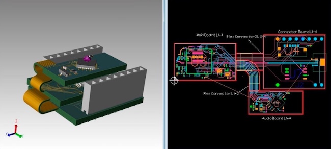
Figure 2. Vizualizing rigid-flex in 3D and 2D environments (Mentor)
7. Manufacturing and assembly for IoT PCB designs
Software that performs design for manufacturability and assembly (DFMA) analysis before a design is sent for fabrication can catch issues such as resist slivers and copper exposure. Panelization considerations and the use of database standards that enable a smoother transfer of design files to the manufacturer should also be part of your design flow.
IoT designs will frequently have to work within extremely thin margins for profitability. Any form of delay or respin can tip such projects into the red.