A PCB designer has a difficult task when it comes to routing a circuit board. Things get a lot more complicated when the design involves high-speed signals. In an effort to help these PCB designers, we have drafted a list of best high-speed PCB routing practices that will assist them in achieving that perfect high-speed design.
In this article, we discuss the following routing practices.
- Route high-speed signals over a solid ground plane
- Avoid hot spots by placing vias in a grid.
- Keep trace bends at 135⁰ instead of 90⁰ avoid acute angles.
- Increase the spacing between traces to avoid crosstalk
- Avoid long stub traces by implementing daisy chain routing
- Do not place any components or vias between differential pairs
- Incorporate length matching to avoid skew between differential pairs
- Do not route signal over a split plane
- Separate analog and digital ground planes to reduce noise
- Split the layouts virtually between analog and digital grounds
- Keep trace width as per the size of discrete component
Route high-speed signals over a solid ground plane
As a rule of thumb, it’s most beneficial to have a common ground plane below signal traces. For best results, a designer should incorporate at least a four-layer PCB. A four-layer PCB allows devoting one of the inner layers to a full ground plane. A ground plane is a sheet of copper, forming one of the layers of the PCB and covering the entire area of one of the layers of the PCB. This ensures minimal impedance between any two ground points in the PCB. This ground plane should never be broken by routing any tracks in it.
When the external layer nearest to the ground plane is used to mount all the high-speed components like RF components using microstrip traces or coplanar traces. The opposite side is used for mounting less critical components. The second inner layer is used for power planes. The power planes are made as large as possible to reduce the impedance.
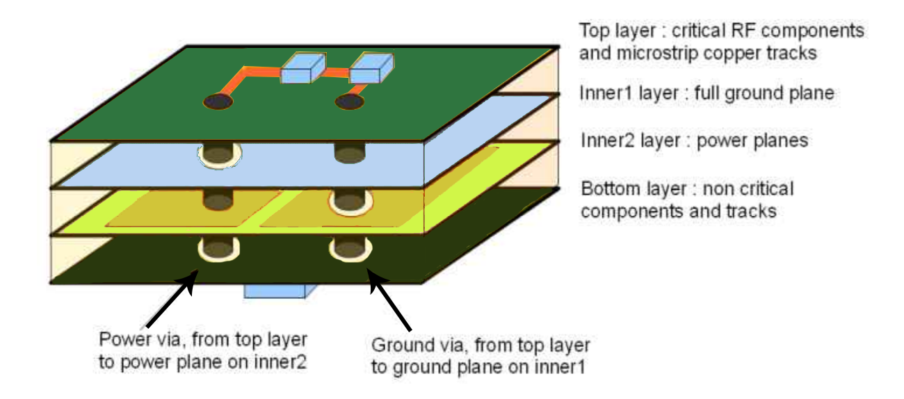 Figure 1: Four-layer PCB structure
A double-sided PCB may be the right choice when it comes to cost minimization. Achieving this is quite difficult. When there is a requirement to route tracks on both sides of the PCB in the same area then a good ground plane is no longer guaranteed. The only solution is then to implement ground planes on both sides of the traces that are interconnected by plenty of vias as shown in figure (2).
Designing a double-sided PCB becomes complex when the ground plane gets shared between the top and bottom layers. The designer should ensure that there is at least a full ground plane under the most critical section. The top side must be used for routing as much as possible with a few traces on the bottom side. Lots of interconnecting vias are needed to interconnect the top and the bottom grounds. Most importantly, traces should never cross the high-speed traces on the opposite side in a two-layer board.
Split ground planes are sometimes implemented in critical cases. For instance, a ground plane for the logic sections and a ground plane for the analog components, connected at a single point.
The concept is to reduce the noise in the analog ground planes. Sadly, it is quite challenging to accurately implement such an idea. In particular, it is then mandatory to route all the traces going from one region to the other exclusively above this interconnecting point as shown in figure (3). If not, then these traces will act as an antenna which will either transmit or receive spurious signals. In most cases, a full single ground is more reliable and provides better results than split grounds, as long as the placement of the components is in proper ground section.
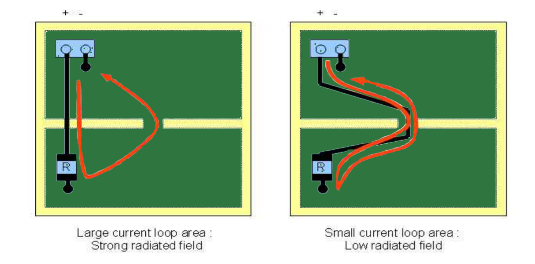
Usually, a split ground plane is avoided, unless there is a specific need like reducing strong ESD risks and reducing analog ground noise.
Avoid hot spots by placing vias in a grid.
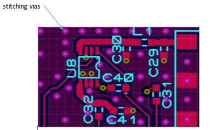
The signal vias produce voids in the power and ground planes. Improper positioning of vias can create plane areas in which the current density is increased. These regions are called hot spots. These hot spots must be avoided. The best solution is to place the vias as shown in figure (4) in a grid that leaves enough space between the vias for the power plane to pass. As a thumb rule, place vias 15 mils apart wherever possible.

Keep 135⁰ trace bends instead of 90⁰ while routing high-speed signals.
The bends should be kept minimum while routing high-speed signals. If the bends are required, then 135° bends should be implemented instead of 90°as shown in figure (5, Right side). At 90 degrees, smooth PCB etching is not guaranteed. Also, very high-speed sharp edges act as an antenna.

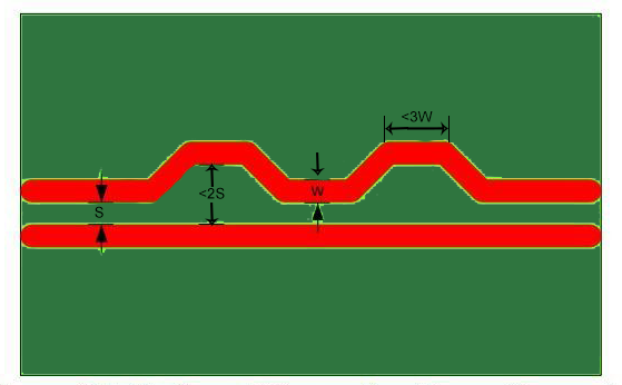
To achieve a specific trace length, serpentine traces are needed as shown in figure (6). A minimum distance of 4 times the trace width must be maintained between adjacent copper in the same trace. Each segment of the bends should be 1.5 times the trace width. Most of the DRCs in CAD tools do not check these minimum distances as the traces are part of the same net.

Increase the distance between the signals outside the bottleneck regions to evade crosstalk.
A minimum distance should be maintained between traces to minimize the crosstalk. The crosstalk level depends on the length and the distance between the two traces. In some areas, the routing of traces reaches a bottleneck where the traces are closer than desired. In such situations, the distance between the signals outside the bottleneck should be increased. Even if the minimum requirement is met, the spacing can be increased a little further.

Avoid long stub traces by implementing daisy chain routing to maintain signal integrity.
The long stub traces may act as antennas and consequently increase problems complying with EMC standards. Stub traces can also create reflections that negatively affect signal integrity. Pull-up or pull-down resistors on high-speed signals are common sources of stubs. If such resistors are required then route the signals as a daisy chain as shown in figure (8).

When routing high-speed differential pairs parallel to each other, a constant distance should be maintained between them. This distance helps to achieve the specified differential impedance. The designer should minimize the area in which the specified spacing is enlarged due to pad entries. The differential pairs should be routed symmetrically.

The designer should not place any components or vias between differential pairs even if the signals are routed symmetrically as shown in figure (10). Placement of components and vias between differential pairs could lead to EMC problems and impedance discontinuities.

Some high-speed differential pairs need serial coupling capacitors. These capacitors should be placed symmetrically. The capacitors and the pads produce impedance discontinuities. Capacitor sizes such as 0402 are preferable over 0603. Larger packages such as 0805 or C-packs must be avoided.

Since the vias introduce an enormous discontinuity in impedance, the number of vias must be reduced and should be placed symmetrically.

While routing a differential pair, both the traces should be routed on the same layer so that the impedance requirements are met as shown in figure (13). Also, the same number of vias should be included in the traces.

Incorporate length matching to achieve tight delay skew between positive and negative signals.
The high-speed interfaces have additional requirements concerning the time of arrival at a destination known as clock skew between different traces and pairs of signals. For instance, in a high-speed parallel bus, all data signals need to arrive within a time period in order to meet the setup and hold time requirements of the receiver. The PCB designer should ensure that such permitted skew is not exceeded. To achieve this requirement, the length matching is necessary.
The differential pair signals demand a very tight delay skew between the positive and negative signal traces. Hence, any length differences should be compensated by using serpentines. The geometry of serpentine traces should be carefully designed as shown in figure (14) to reduce impedance discontinuity.
The designer should place the serpentine traces at the root of the length mismatch. This ensures that the positive and negative signal components are propagated synchronously over the connection as shown in figure (15).

The bends are usually the source of length mismatches. The compensation should be planted very close to the bend with a maximum distance of 15mm as shown in the below figure (16).

Generally, two bends compensate each other. If the bends are closer than 15mm then no additional compensation with serpentines is necessary. The signals should not traverse asynchronously over a distance of more than 15mm.

The mismatches in each segment of a differential pair connection should be matched individually. In figure (18) shown below, the vias separate the differential pair into two segments. The bends need to be compensated individually here. This ensures that the positive and negative signals are propagated synchronously through the vias. The DRC overlooks this violation since it only checks the length difference over the whole connection.

The signal speed is not the same in all the layers of a PCB. Since it is hard to figure out the difference, it is preferable to route signals on the same layer if they need to be matched.

Some of the CAD tools also consider the trace length inside a pad to its total length. The figure shown below depicts two layouts which are similar from an electrical point of view.
In figure (20) on the left, the traces inside the capacitor pads do not have an equal length. Even though the signals are not using the internal traces, some CAD tools consider this as part of the length calculation and display a length difference between the positive and negative signals. In order to minimize this, ensure that the pad entry is equal for both signals.
In the same way, some CAD tools do not consider the length of vias when calculating the total length. Since differential pairs should have the same amount of vias in both traces, the error does not affect the length matching. However, it can affect calculations for matching two differential pairs or the matching of parallel buses.

Asymmetric breakout of differential pair signal is preferred as shown in figure (21), wherever possible in order to avoid the serpentine traces.

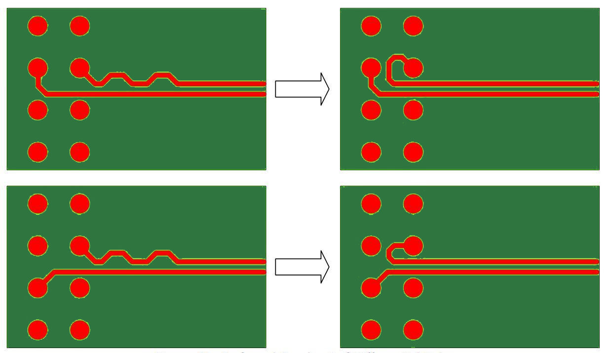
Small loops can be included for the shorter trace instead of serpentine traces if there is enough space between pads. This is generally preferred over a serpentine trace.
Do not route signal over a split plane
An incorrect signal return path results in noise coupling and EMI issues. The designer should always think of the signal return path when routing a signal. The power rails and low-speed signals take the shortest return current path as shown in figure (23). In contrast to this, the return current of high-speed signals tries to follow the signal path.

A signal should not be routed over a split plane as the return path is not able to follow the signal trace. Refer figure (24). If a plane is split between a sink and source, route the signal trace around it. If the forward and return paths of a signal are separated, the area between them acts as a loop antenna.
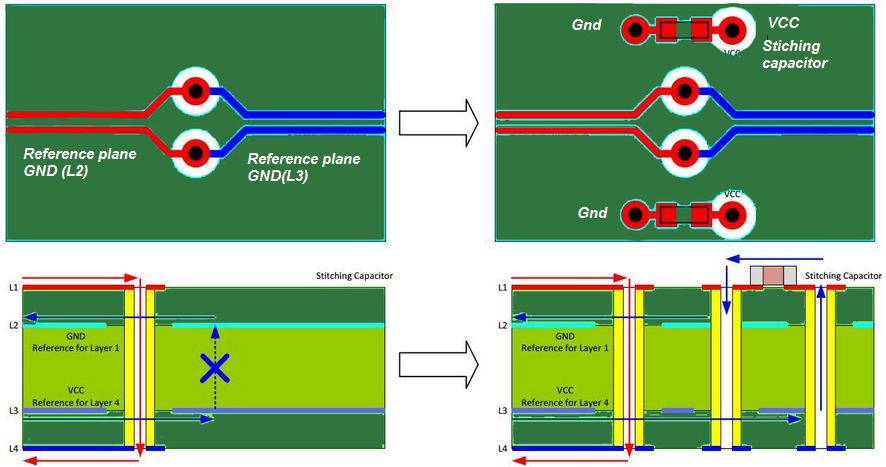
Stitching capacitors should be incorporated if a signal needs to be routed over two different reference planes. The stitching capacitor enables the return current to travel from one reference plane to the other. The capacitor should be placed close to the signal path so that the distance between the forward and return path are kept small. Generally, the values of stitching capacitors are between 10nF and 100nF.

In general, plane obstructions and plane slots must be avoided. If it is really necessary to route over such obstruction then stitching capacitors should be used as shown in figure (25).

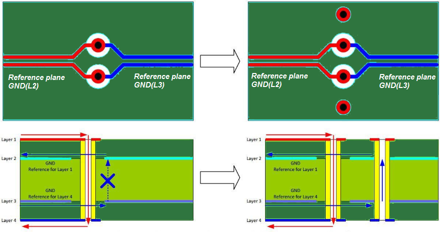
The designer should look out for voids (no copper area) in reference planes while routing high-speed signals. Voids in reference planes are generated when placing vias close together as shown in figure (25). Large void areas should be avoided by ensuring adequate separation between vias. It is better to place fewer ground and power vias in order to reduce via voids.

The return path should be considered at the source and sink of a signal. In figure (27) shown below, the left design is considered to be a bad design. Since there is only one single ground via on the source side, the return current cannot travel back over the reference ground plane as intended. The return path is the ground connection present on the top layer instead. The problem in hand is that the impedance of the signal trace is calculated as referenced to the ground plane and not to the ground trace on the top layer. Hence, it is essential to place ground vias at the source and sink side of the signal. This allows the return current to travel back on the ground plane as shown in figure (27) on the right.

When a power plane is considered as a reference to a signal, then the signal should be able to propagate back over the power plane. The signals are referenced to ground in the source and sink. To switch the reference to the power plane, stitching capacitors should be incorporated at the sink and source. If the sink and source are utilizing the same power rail for their supply, then the bypass capacitors can act as stitching capacitors if they are placed close to the signal start/exit point as shown in figure (28). The ideal value for the stitching capacitor is between 10nF and 100nF.

When a differential signal switches a layer, the reference ground plane will also be switched. Hence, stitching vias should be added close to the layer change vias as shown in figure (29) on the right. This permits the return current to change the ground plane. When dealing with differential signals, the switching ground vias should be placed symmetrically.
When a signal switches to a different layer that has a different reference plane then stitching capacitors should be implemented. This permits the return current to flow from the ground to the power plane through the stitching capacitor as shown in figure 30 on the right. Also, the stitching capacitor placement and routing should be symmetrical when differential pairs are considered.
The designer should not route high-speed signals on the edge of the reference planes or close to PCB borders. This can have an adverse impact on the trace impedance.

Separate Analog and Digital ground planes to reduce noise
Defining separate Analog and Digital ground sections approach makes it easy in the schematic to determine which components and pins should be connected to the digital ground and which ones to the analog ground section. These kinds of designs can be routed by placing two different ground planes as reference. The two planes should be placed accurately. The digital and analog components should be placed underneath the respective sections as shown in figure (32, right).

The mixed-signal circuits require the analog and digital ground connected at a single point. In the schematics, it is always recommended to place ferrite beads or zero-ohm resistors between the analog and digital sections. The merging of the digital and analog ground should be placed close to the integrated circuit. In a mixed-signal design that has split planes, the digital signal should not be routed over an analog ground plane and the analog signal should not be routed over the digital ground plane.

Split the layouts virtually between analog and digital grounds.
In the virtual split approach, the analog and digital ground are not separated in the schematic diagram. Also, the two ground domains are not electrically separated in the layout either. Interestingly, the layout is split virtually, i.e., an imaginary separation is drawn between the analog and digital ground. The components should be placed carefully considering the correct side of the virtually split planes.

The designer should keep in mind the virtual line between the two ground domains during the high-speed PCB routing process. Neither the digital nor the analog signal trace is allowed to cross the virtual split line. The virtual split line should not have a complicated shape since there is no plane obstruction to keep the analog and digital return current separated.
Learn How To Breakout a .5mm BGA
Best high-speed performance is achieved if the width of the component is close to the track width.
Let’s understand our last high-speed PCB routing tip. The board design begins with the schematic, specifically with the selection of the components. The surface-mount devices (SMD) are preferred since smaller components and shorter wires result in more stable high-speed performances.
Choosing the package can get tricky sometimes. One beneficial criterion is to look at the track width calculated for a 50-ohm impedance. The best high-speed performances are usually accomplished if the width of the component is close to track width. This will lower the impedance matching issues between the track and the component pad.
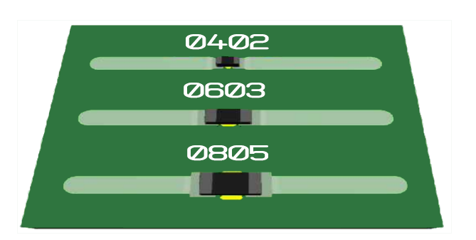
The impedance mismatches can be reduced by selecting those components that have a package that is almost the same size as of the calculated track width. The test points should be planned at the schematic phase.
