
The definition of a multilayer circuit board is a PCB made of three or more layers of conductive copper foil. They appear as several layers of double-sided circuit boards, laminated and glued together, with thermal insulation between them. All electrical connections between layers are made through holes, such as plated through holes, blind vias, and buried vias. From a technical perspective, multilayer circuit boards offer several design advantages.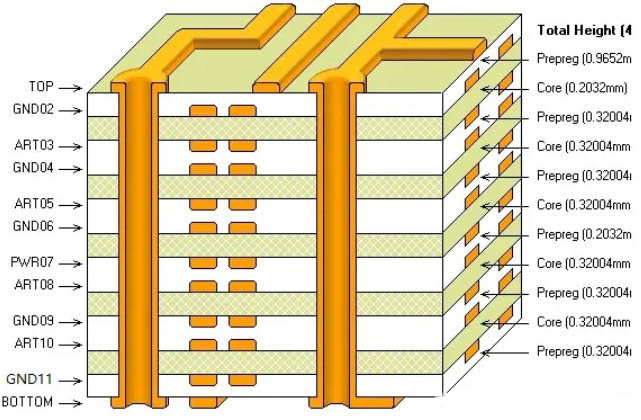
1. Small size: One of the most prominent and praiseworthy benefits of using multi-layer PCB is its size. Due to their multi-layer design, multi-layer PCBs are inherently smaller than other PCBs with similar functionality. Since the current trend is towards smaller, smaller yet more powerful gadgets, this brings major benefits to modern electronics.
2. Lightweight structure: The smaller the PCB, the lighter it is, especially since the multiple connectors required to interconnect separate single- and double-layer PCBs are eliminated in favor of a multi-layer design. Again, this is advantageous for modern electronics, which are better suited for mobility.
3. High quality: Due to the amount of work and planning required to create a multi-layer PCB, these types of PCBs tend to be better in quality than single- and double-layer PCBs. As a result, they also tend to be more reliable.
4. Enhanced durability: Multi-layer PCBs tend to be durable by nature. Not only do these multi-layer PCBs have to support their own weight, they also have to be able to withstand the heat and pressure that holds them together. On top of these factors, multilayer PCBs use multiple layers of insulation between circuit layers and bind them all together with prepreg adhesive and protective materials.
5. More powerful: Multi-layer PCBs are extremely high-density components that integrate multiple layers into a single PCB. These nearly quarters make the board more connected, and its inherent electrical properties allow it to achieve greater capacity and speed despite its smaller size.
6. Single connection point: Multi-layer PCB is designed as a single unit rather than in series with other PCB components. As a result, they have only one connection point instead of the multiple connection points required using multiple single-layer PCBs. This is particularly beneficial for small electronics and gadgets designed to minimize size and weight.