
Corresponding inspections are required before and after the complete PCBA processing is completed. So, how to effectively inspect after SMT chip processing?
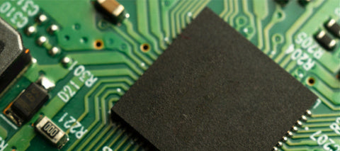
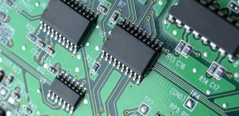
1. Check the layout of the pcb module board for foreign matter residues, PCB scratches and other undesirable phenomena.
2. The inspection direction is moved from left to right and from top to bottom, and the mounted copper base pcb are inspected one by one.
3. The components should not be missing, wrongly installed, empty welding, etc.
4. The polarity of the components cannot be reversed.
5. The pin displacement of IC, exclusion, transistor, etc. cannot exceed 1/4 of the pad width.
6. The displacement of the Chip component cannot exceed 1/4 of the width of the pad in the parallel and vertical directions.
7. Hold the edge of the high volume pcb and gently place it on the conveyor belt of the reflow soldering machine. Be careful not to drop it from a high place to prevent the components from falling off.
8. Detect the bad small batch pcb, paste the sign paper, and trim and adjust it in time.
9. Other precautions: You must wear an anti-static wrist strap. Take the edge of the PCB during operation, and do not touch the surface of the smt pcb with your hands to prevent damage to the solder paste printed on the pad; during the mounting process, add components Be sure to pay attention to the model, specification, polarity and direction of the components.