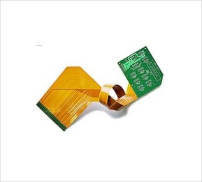
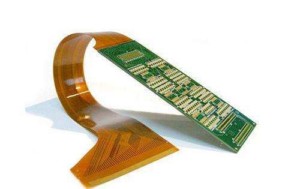
1. Bend Radius:
- **Minimum Bend Radius:** Define the minimum bend radius based on the flexibility of the materials used in the flex PCB to prevent stress on the traces and components during bending.

2. Trace Width and Spacing:
- **Wide Traces:** Use wider traces to reduce resistance and accommodate potential bending stresses.- **Spacing:** Maintain appropriate clearance and spacing between traces to prevent short circuits, especially in areas prone to bending.
3. Component Placement:
- **SMD Components:** Opt for surface-mount devices (SMDs) to reduce stress on component leads during flexing.- **Avoidance of Critical Components:** Place critical components away from areas where bending is frequent to prevent damage.
4. Pad and Via Placement:
- **Pad Size:** Use larger pad sizes for vias and component connections to enhance soldering reliability on flexible substrates.- **Via Orientation:** Avoid placing vias in areas with high bending stress to prevent cracking and ensure signal integrity.
5. Cutouts and Stiffeners:
- **Stiffeners:** Incorporate stiffeners or reinforcement materials in areas where components are mounted or where additional support is needed during bending.- **Cutouts:** Design cutouts in the flexible material to accommodate connectors or specific mechanical requirements.
6. Signal Integrity:
- **Impedance Control:** Maintain consistent impedance profiles along signal traces to prevent signal degradation and reflections in bend areas.- **Cross-Talk Mitigation:** Implement signal shielding and proper isolation to reduce cross-talk in flexible circuits.
7. Material Selection:
- **Flex Material Properties:** Choose flexible substrate materials with appropriate mechanical properties, such as tensile strength and elongation, to withstand bending cycles.- **Adhesive Selection:** Select adhesives that can withstand bending without delaminating to ensure long-term reliability.
8. Flex Region Identification:
- **Clearly Define Flex Region:** Clearly mark flexible areas on the PCB design to indicate where bending is allowed and where components should not be placed.

9. Test Points:
- **Accessibility:** Include test points along the flex PCB for testing and debugging purposes, ensuring that access is not compromised by bending or flexing.By adhering to these flex PCB design rules and considerations, can create robust and functional flexible circuits that meet the required specifications, withstand bending cycles, and maintain reliable performance in various applications.

